ISL6210CRZ Intersil, ISL6210CRZ Datasheet
ISL6210CRZ
Specifications of ISL6210CRZ
Available stocks


Related parts for ISL6210CRZ

ISL6210CRZ Summary of contents
Page 1
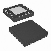
... MARKING (°C) ISL6210CRZ 62 10CRZ -10 to +100 16 Ld 4x4 QFN L16.4x4 ISL6210CRZ-T* 62 10CRZ -10 to +100 16 Ld 4x4 QFN L16.4x4 *Please refer to TB347 for details on reel specifications. NOTE: These Intersil Pb-free plastic packaged products employ special Pb-free material sets, molding compounds/die attach materials, and 100% matte tin plate plus anneal (e3 termination finish, which is RoHS compliant and compatible with both SnPb and Pb-free soldering operations) ...
Page 2
Pinout Block Diagram EN FCCM VCC 4.25k PWM1 4k CONTROL VCC LOGIC 4.25k PWM2 4k GND 2 ISL6210 ISL6210 (16 LD 4X4 QFN) TOP VIEW GND 1 12 UGATE1 LGATE1 2 11 BOOT1 GND 10 PVCC ...
Page 3
Typical Application - Multiphase Converter Using ISL6210 Gate Drivers FB COMP VCC VSEN ISEN1 PWM1 PGOOD EN PWM2 ISEN2 MAIN CONTROL ISL62xx VID ISEN3 FCCM PWM3 PWM4 ISEN4 GND EN 3 ISL6210 BOOT1 +5V UGATE1 VCC PHASE1 FCCM LGATE1 EN ...
Page 4
... QFN Package . . . . . . . . . . . . . . . . . . Maximum Junction Temperature . . . . . . . . . . . . . . . . . . . . . . +150° -0. (DC) Maximum Storage Temperature Range . . . . . . . . . .-65°C to +150°C -0. (<10ns) Pb-Free Reflow Profile .see link below http://www.intersil.com/pbfree/Pb-FreeReflow.asp - 0.3V (DC BOOT Recommended Operating Conditions BOOT Ambient Temperature Range .-10°C to +100°C Maximum Operating Junction Temperature +125°C Supply Voltage, VCC . . . . . . . . . . . . . . . . . . . . . . . . . . . . . 5V ± ...
Page 5
Electrical Specifications These specifications apply for T MIN and/or MAX limits are 100% tested at +25°C, unless otherwise specified. Temperature limits established by characterization and are not production tested. PARAMETER OUTPUT Upper Drive Source Resistance Upper Drive Source Current (Note ...
Page 6
... MOSFET can cause gross current measurement inaccuracies. Three-State PWM Input A unique feature of the ISL6210 and other Intersil drivers is the addition of a shutdown window to the PWM input. If the PWM signal enters and remains within the shutdown window for a set holdoff time, the output drivers are disabled and both MOSFET gates are pulled and held low ...
Page 7
During turn-off of the lower MOSFET, the LGATE voltage is monitored until it reaches a 1V threshold, at which time the UGATE is released to rise. Adaptive shoot-through circuitry monitors the upper MOSFET gate-to-source voltage during UGATE turn-off. Once the ...
Page 8
Q = 100nC 0.6 GATE 0.4 0.2 20nC 0.0 0.0 0.1 0.2 0.3 0.4 0.5 ΔV BOOT_CAP FIGURE 4. BOOTSTRAP CAPACITANCE vs BOOT RIPPLE VOLTAGE Power Dissipation Package power dissipation is mainly a ...
Page 9
... Accordingly, the reader is cautioned to verify that data sheets are current before placing orders. Information furnished by Intersil is believed to be accurate and reliable. However, no responsibility is assumed by Intersil or its subsidiaries for its use; nor for any infringements of patents or other rights of third parties which may result from its use ...
Page 10
Package Outline Drawing L16.4x4 16 LEAD QUAD FLAT NO-LEAD PLASTIC PACKAGE Rev 6, 02/08 4.00 6 PIN 1 INDEX AREA 0.15 (4X) TOP VIEW ( TYP ) ( TYPICAL RECOMMENDED LAND PATTERN 10 ...