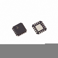
ISL6614CRZ-T Intersil, ISL6614CRZ-T Datasheet - Page 9

ISL6614CRZ-T
Manufacturer Part Number
ISL6614CRZ-T
Description
IC DRIVER DUAL SYNC BUCK 16-QFN
Manufacturer
Intersil
Datasheet
1.ISL6614CBZ.pdf
(12 pages)
Specifications of ISL6614CRZ-T
Configuration
High and Low Side, Synchronous
Input Type
PWM
Delay Time
10.0ns
Current - Peak
1.25A
Number Of Configurations
2
Number Of Outputs
4
High Side Voltage - Max (bootstrap)
36V
Voltage - Supply
10.8 V ~ 13.2 V
Operating Temperature
0°C ~ 85°C
Mounting Type
Surface Mount
Package / Case
16-VQFN Exposed Pad, 16-HVQFN, 16-SQFN, 16-DHVQFN
Lead Free Status / RoHS Status
Lead free / RoHS Compliant
Available stocks
Company
Part Number
Manufacturer
Quantity
Price
Company:
Part Number:
ISL6614CRZ-T
Manufacturer:
INTERSIL/PB-FREE
Quantity:
11 994
Part Number:
ISL6614CRZ-T
Manufacturer:
INTERSIL
Quantity:
20 000
Schottky diode that is used in some systems for protecting
the load from reversed output voltage events.
In addition, more than 400mV hysteresis also incorporates
into the three-state shutdown window to eliminate PWM
input oscillations due to the capacitive load seen by the
PWM input through the body diode of the controller’s PWM
output when the power-up and/or power-down sequence of
bias supplies of the driver and PWM controller are required.
Power-On Reset (POR) Function
During initial startup, the VCC voltage rise is monitored.
Once the rising VCC voltage exceeds 9.8V (typically),
operation of the driver is enabled and the PWM input signal
takes control of the gate drives. If VCC drops below the
falling threshold of 7.6V (typically), operation of the driver is
disabled.
Pre-POR Overvoltage Protection
Prior to VCC exceeding its POR level, the upper gate is held
low and the lower gate is controlled by the overvoltage
protection circuits during initial startup. The PHASE is
connected to the gate of the low side MOSFET (LGATE),
which provides some protection to the microprocessor if the
upper MOSFET(s) is shorted during initial startup. For
complete protection, the low side MOSFET should have a
gate threshold well below the maximum voltage rating of the
load/microprocessor.
When VCC drops below its POR level, both gates pull low
and the Pre-POR overvoltage protection circuits are not
activated until VCC resets.
Internal Bootstrap Device
Both drivers feature an internal bootstrap Schottky diode.
Simply adding an external capacitor across the BOOT and
PHASE pins completes the bootstrap circuit. The bootstrap
function is also designed to prevent the bootstrap capacitor
from overcharging due to the large negative swing at the
trailing-edge of the PHASE node. This reduces voltage
stress on the boot to phase pins.
The bootstrap capacitor must have a maximum voltage
rating above UVCC + 5V and its capacitance value can be
chosen from Equation 1:
where Q
at V
MOSFETs per channel. The ΔV
the allowable droop in the rail of the upper gate drive.
As an example, suppose two IRLR7821 FETs are chosen as
the upper MOSFETs. The gate charge, Q
C
Q
BOOT_CAP
GATE
GS1
=
gate-source voltage and N
G1
Q
----------------------------------- - N
G1
is the amount of gate charge per upper MOSFET
≥
V
------------------------------------- -
ΔV
•
GS1
PVCC
BOOT_CAP
Q
GATE
•
Q1
9
BOOT_CAP
Q1
is the number of control
G
term is defined as
, from the data
(EQ. 1)
ISL6614
sheet is 10nC at 4.5V (V
Q
assume a 200mV droop in drive voltage over the PWM
cycle. We find that a bootstrap capacitance of at least
0.267µF is required.
Gate Drive Voltage Versatility
The ISL6614 provides the user flexibility in choosing the
gate drive voltage for efficiency optimization. The ISL6614
ties the upper and lower drive rails together. Simply applying
a voltage from 5V up to 12V on PVCC sets both gate drive
rail voltages simultaneously. Connecting a SOT-23 package
type of dual Schottky diodes from the VCC to BOOT1 and
BOOT2 can bypass the internal bootstrap devices of both
upper gates so that the part can operate as a dual ISL6612
driver, which has a fixed VCC (12V typically) on the upper
gate and a programmable lower gate drive voltage.
Over-Temperature Protection (OTP)
When the junction temperature of the IC exceeds +150°C
(typically), both upper and lower gates turn off. The driver
stays off and does not return to normal operation until its
junction temperature comes down below +108°C (typically).
For high frequency applications, applying a lower voltage to
PVCC helps reduce the power dissipation and lower the
junction temperature of the IC. This method reduces the risk
of tripping OTP.
Power Dissipation
Package power dissipation is mainly a function of the
switching frequency (f
external gate resistance, and the selected MOSFET’s
internal gate resistance and total gate charge. Calculating
the power dissipation in the driver for a desired application is
critical to ensure safe operation. Exceeding the maximum
allowable power dissipation level will push the IC beyond the
maximum recommended operating junction temperature of
+125°C. The maximum allowable IC power dissipation for
GATE
FIGURE 2. BOOTSTRAP CAPACITANCE vs BOOT RIPPLE
1.6
1.4
1.2
1.0
0.8
0.6
0.4
0.2
0.0
is calculated to be 53nC for PVCC = 12V. We will
0.0
20nC
0.1
VOLTAGE
0.2
50nC
Q
SW
GATE
0.3
GS
), the output drive impedance, the
= 100nC
) gate-source voltage. Then the
ΔV
0.4
BOOT_CAP
0.5
0.6
(V)
0.7
0.8
May 5, 2008
0.9
FN9155.5
1.0


