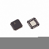
ISL6614CRZ-T Intersil, ISL6614CRZ-T Datasheet - Page 7

ISL6614CRZ-T
Manufacturer Part Number
ISL6614CRZ-T
Description
IC DRIVER DUAL SYNC BUCK 16-QFN
Manufacturer
Intersil
Datasheet
1.ISL6614CBZ.pdf
(12 pages)
Specifications of ISL6614CRZ-T
Configuration
High and Low Side, Synchronous
Input Type
PWM
Delay Time
10.0ns
Current - Peak
1.25A
Number Of Configurations
2
Number Of Outputs
4
High Side Voltage - Max (bootstrap)
36V
Voltage - Supply
10.8 V ~ 13.2 V
Operating Temperature
0°C ~ 85°C
Mounting Type
Surface Mount
Package / Case
16-VQFN Exposed Pad, 16-HVQFN, 16-SQFN, 16-DHVQFN
Lead Free Status / RoHS Status
Lead free / RoHS Compliant
Available stocks
Company
Part Number
Manufacturer
Quantity
Price
Company:
Part Number:
ISL6614CRZ-T
Manufacturer:
INTERSIL/PB-FREE
Quantity:
11 994
Part Number:
ISL6614CRZ-T
Manufacturer:
INTERSIL
Quantity:
20 000
Functional Pin Description
PACKAGE PIN
SOIC
10
11
12
13
14
1
2
3
4
5
6
7
8
9
-
-
NUMBER
DFN
5, 8
15
16
10
11
12
13
14
17
1
2
3
4
6
7
9
SYMBOL
PHASE2
UGATE2
UGATE1
PHASE1
LGATE1
LGATE2
BOOT2
BOOT1
PWM1
PWM2
PVCC
PGND
GND
VCC
PAD
PIN
N/C
The PWM signal is the control input for the Channel 1 driver. The PWM signal can enter three distinct states during
operation, see “Three-State PWM Input” on page 8 for further details. Connect this pin to the PWM output of the
controller.
The PWM signal is the control input for the Channel 2 driver. The PWM signal can enter three distinct states during
operation, see see “Three-State PWM Input” on page 8 for further details. Connect this pin to the PWM output of the
controller.
Bias and reference ground. All signals are referenced to this node.
Lower gate drive output of Channel 1. Connect to gate of the low-side power N-Channel MOSFET.
This pin supplies power to both the lower and higher gate drives in ISL6614. Its operating range is +5V to 12V.
Place a high quality low ESR ceramic capacitor from this pin to GND.
It is the power ground return of both low gate drivers.
No Connection.
Lower gate drive output of Channel 2. Connect to gate of the low-side power N-Channel MOSFET.
Connect this pin to the SOURCE of the upper MOSFET and the DRAIN of the lower MOSFET in Channel 2. This
pin provides a return path for the upper gate drive.
Upper gate drive output of Channel 2. Connect to gate of high-side power N-Channel MOSFET.
Floating bootstrap supply pin for the upper gate drive of Channel 2. Connect the bootstrap capacitor between this
pin and the PHASE2 pin. The bootstrap capacitor provides the charge to turn on the upper MOSFET. See the
“Internal Bootstrap Device” on page 9 for guidance in choosing the capacitor value.
Floating bootstrap supply pin for the upper gate drive of Channel 1. Connect the bootstrap capacitor between this
pin and the PHASE1 pin. The bootstrap capacitor provides the charge to turn on the upper MOSFET. See “Internal
Bootstrap Device” on page 9 for guidance in choosing the capacitor value.
Upper gate drive output of Channel 1. Connect to gate of high-side power N-Channel MOSFET.
Connect this pin to the SOURCE of the upper MOSFET and the DRAIN of the lower MOSFET in Channel 1. This
pin provides a return path for the upper gate drive.
Connect this pin to a +12V bias supply. It supplies power to internal analog circuits. Place a high quality low ESR
ceramic capacitor from this pin to GND.
Connect this pad to the power ground plane (GND) via thermally enhanced connection.
7
ISL6614
FUNCTION
May 5, 2008
FN9155.5


