ISL6208IRZ-T Intersil, ISL6208IRZ-T Datasheet

IC MOSFET DRVR SYNC BUCK 8-QFN

ISL6208IRZ-T

Manufacturer Part Number
ISL6208IRZ-T
Description
IC MOSFET DRVR SYNC BUCK 8-QFN
Manufacturer
Intersil
Datasheet

Specifications of ISL6208IRZ-T

Configuration
High and Low Side, Synchronous
Input Type
PWM
Delay Time
20ns
Current - Peak
2A
Number Of Configurations
1
Number Of Outputs
2
High Side Voltage - Max (bootstrap)
33V
Voltage - Supply
4.5 V ~ 5.5 V
Operating Temperature
-40°C ~ 100°C
Mounting Type
Surface Mount
Package / Case
8-VQFN
Lead Free Status / RoHS Status
Lead free / RoHS Compliant
High Voltage Synchronous Rectified Buck
MOSFET Driver
The ISL6208 is a high frequency, dual MOSFET driver,
optimized to drive two N-Channel power MOSFETs in a
synchronous-rectified buck converter topology. It is
especially suited for mobile computing applications that
require high efficiency and excellent thermal performance.
This driver, combined with an Intersil multiphase Buck PWM
controller, forms a complete single-stage core-voltage
regulator solution for advanced mobile microprocessors.
The ISL6208 features 4A typical sinking current for the lower
gate driver. This current is capable of holding the lower
MOSFET gate off during the rising edge of the Phase node.
This prevents shoot-through power loss caused by the high
dv/dt of phase voltages. The operating voltage matches the
30V breakdown voltage of the MOSFETs commonly used in
mobile computer power supplies.
The ISL6208 also features a three-state PWM input that,
working together with Intersil’s multiphase PWM controllers,
will prevent negative voltage output during CPU shutdown.
This feature eliminates a protective Schottky diode usually
seen in a microprocessor power systems.
MOSFET gates can be efficiently switched up to 2MHz using
the ISL6208. Each driver is capable of driving a 3000pF load
with propagation delays of 8ns and transition times under
10ns. Bootstrapping is implemented with an internal
Schottky diode. This reduces system cost and complexity,
while allowing the use of higher performance MOSFETs.
Adaptive shoot-through protection is integrated to prevent
both MOSFETs from conducting simultaneously.
A diode emulation feature is integrated in the ISL6208 to
enhance converter efficiency at light load conditions. This
feature also allows for monotonic start-up into pre-biased
outputs. When diode emulation is enabled, the driver will
allow discontinuous conduction mode by detecting when the
inductor current reaches zero and subsequently turning off
the low side MOSFET gate.
®
1
Data Sheet
1-888-INTERSIL or 1-888-468-3774
CAUTION: These devices are sensitive to electrostatic discharge; follow proper IC Handling Procedures.
Features
• Dual MOSFET Drives for Synchronous Rectified Bridge
• Adaptive Shoot-Through Protection
• 0.5Ω On-Resistance and 4A Sink Current Capability
• Supports High Switching Frequency up to 2MHz
• Three-State PWM Input for Power Stage Shutdown
• Internal Bootstrap Schottky Diode
• Low Bias Supply Current (5V, 80µA)
• Diode Emulation for Enhanced Light Load Efficiency and
• VCC POR (Power-On-Reset) Feature Integrated
• Low Three-State Shutdown Holdoff Time (Typical 160ns)
• Pin-to-Pin Compatible with ISL6207
• QFN Package:
• Pb-Free available (RoHS compliant)
Applications
• Core Voltage Supplies for Intel® and AMD® Mobile
• High Frequency Low Profile DC/DC Converters
• High Current Low Output Voltage DC/DC Converters
• High Input Voltage DC/DC Converters
Related Literature
• Technical Brief TB363 “Guidelines for Handling and
• Technical Brief TB389 “PCB Land Pattern Design and
• Technical Brief TB447 “Guidelines for Preventing
- Fast output rise and fall time
- Low propagation delay
Pre-Biased Start-Up Applications
- Compliant to JEDEC PUB95 MO-220
- Near Chip Scale Package footprint, which improves
Microprocessors
Processing Moisture Sensitive Surface Mount Devices
(SMDs)”
Surface Mount Guidelines for MLFP Packages”
Boot-to-Phase Stress on Half-Bridge MOSFET Driver ICs”
QFN - Quad Flat No Leads - Package outline
PCB efficiency and has a thinner profile
August 7, 2008
All other trademarks mentioned are the property of their respective owners.
|
Intersil (and design) is a registered trademark of Intersil Americas Inc.
Copyright © Intersil Americas Inc. 2004-2008. All Rights Reserved
ISL6208
FN9115.3

Related parts for ISL6208IRZ-T

ISL6208IRZ-T Summary of contents

Page 1

... CAUTION: These devices are sensitive to electrostatic discharge; follow proper IC Handling Procedures. | 1-888-INTERSIL or 1-888-468-3774 Intersil (and design registered trademark of Intersil Americas Inc. Copyright © Intersil Americas Inc. 2004-2008. All Rights Reserved All other trademarks mentioned are the property of their respective owners. ISL6208 ...

Page 2

... ISL6208IBZ* (Note) ISL62 08IBZ ISL6208IR* 208I ISL6208IRZ* (Note) 81RZ * Add “-T” suffix for Tape and Reel. Please refer to TB347 for details on reel specifications. NOTE: These Intersil Pb-free plastic packaged products employ special Pb-free material sets, molding compounds/die attach materials, and 100% matte tin plate plus anneal (e3 termination finish, which is RoHS compliant and compatible with both SnPb and Pb-free soldering operations) ...

Page 3

... ISL6208 Thermal Information Thermal Resistance (Typical) SOIC Package (Note QFN Package (Notes 3, 4 -0. (DC) Maximum Storage Temperature Range . . . . . . . . . .-65°C to +150°C -0. (<10ns) Pb-Free Reflow Profile .see link below http://www.intersil.com/pbfree/Pb-FreeReflow.asp - 0.3V (DC BOOT BOOT SYMBOL TEST CONDITIONS I PWM pin floating, V VCC FCCM ...

Page 4

Electrical Specifications Recommended Operating Conditions, Unless Otherwise Noted. Parameters with MIN and/or MAX limits are 100% tested at +25°C, unless otherwise specified. Temperature limits established by characterization and are not production tested. (Continued) PARAMETER LGATE Rise Time (Note 5) UGATE ...

Page 5

Typical Application with 2-Phase Converter +5V +5V FB COMP VCC VSEN PWM1 PWM2 PGOOD FCCM MAIN CONTROL ISEN1 VID ISEN2 FS DACOUT GND 5 ISL6208 +5V V BAT VCC BOOT UGATE FCCM PWM PHASE DRIVE ISL6208 LGATE THERMAL PAD +5V ...

Page 6

Timing Diagram t PWM PDHU t PDLU t RU UGATE LGATE PDLL Functional Pin Description UGATE (Pin 1 for SOIC-8, Pin 8 for QFN) The UGATE pin is the upper gate drive output. Connect to the ...

Page 7

Typical Performance Waveforms FIGURE 2. LOAD TRANSIENT (0 - 30A, 3-PHASE) FIGURE 4. DCM TO CCM TRANSITION AT NO LOAD FIGURE 6. PRE-BIASED START-UP IN CCM MODE 7 ISL6208 FIGURE 3. LOAD TRANSIENT (30 - 0A, 3-PHASE) FIGURE 5. CCM ...

Page 8

... The turn-OFF of the low side MOSFET can cause gross current measurement inaccuracies. Three-State PWM Input A unique feature of the ISL6208 and other Intersil drivers is the addition of a shutdown window to the PWM input. If the PWM signal enters and remains within the shutdown window for a set holdoff time, the output drivers are disabled and both MOSFET gates are pulled and held low ...

Page 9

... Input capacitors should be placed as close to the DRAIN of the upper FET and the SOURCE of the lower FET as thermally possible. Note: Refer to Intersil Tech Brief TB447 for more information. Thermal Management For maximum thermal performance in high current, high switching frequency applications, connecting the thermal ...

Page 10

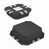
Package Outline Drawing L8.3x3 8 LEAD QUAD FLAT NO-LEAD PLASTIC PACKAGE Rev 2, 3/07 3.00 6 PIN 1 INDEX AREA (4X) 0.15 TOP VIEW ( 2. 60 TYP ) ( TYPICAL RECOMMENDED LAND PATTERN 10 ISL6208 A ...

Page 11

... Accordingly, the reader is cautioned to verify that data sheets are current before placing orders. Information furnished by Intersil is believed to be accurate and reliable. However, no responsibility is assumed by Intersil or its subsidiaries for its use; nor for any infringements of patents or other rights of third parties which may result from its use ...

Related keywords