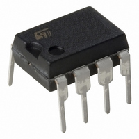
L6385 STMicroelectronics, L6385 Datasheet - Page 2

L6385
Manufacturer Part Number
L6385
Description
IC DRIVER HI/LO SIDE HV 8MINIDIP
Manufacturer
STMicroelectronics
Type
Driverr
Datasheet
1.L6385.pdf
(9 pages)
Specifications of L6385
Configuration
Half Bridge
Input Type
Non-Inverting
Delay Time
110ns
Current - Peak
400mA
Number Of Configurations
1
Number Of Outputs
2
High Side Voltage - Max (bootstrap)
600V
Voltage - Supply
17V
Operating Temperature
-40°C ~ 125°C
Mounting Type
Through Hole
Package / Case
8-DIP (0.300", 7.62mm)
Rise Time
50 ns
Fall Time
30 ns
Supply Current
0.32 mA
Maximum Power Dissipation
750 mW
Maximum Operating Temperature
+ 125 C
Mounting Style
Through Hole
Minimum Operating Temperature
- 45 C
Number Of Drivers
2
For Use With
497-5492 - EVAL BOARD FOR L6384/L6385/L6386
Lead Free Status / RoHS Status
Contains lead / RoHS non-compliant
Other names
497-3649
Available stocks
Company
Part Number
Manufacturer
Quantity
Price
Part Number:
L6385
Manufacturer:
ST
Quantity:
20 000
Part Number:
L6385D013TR
Manufacturer:
ST
Quantity:
20 000
Company:
Part Number:
L6385ED
Manufacturer:
STMicroelectronics
Quantity:
220
L6385
ABSOLUTE MAXIMUM RATINGS
Note: ESD immunity for pins 6, 7 and 8 is guaranteed up to 900V (Human Body Model)
PIN CONNECTION
THERMAL DATA
PIN DESCRIPTION
(*) The circuit guarantees 0.3V maximum on the pin (@ I
2/9
and the source of the external MOSFET normally used to hold the pin low.
N.
1
2
3
4
5
6
7
8
dVout/dt
Symbol
Symbol
R
Vboot
Vhvg
Vout
Vlvg
th j-amb
Ptot
Vcc
Ts
Vi
Tj
HVG (*)
LVG (*)
Name
VOUT
Vboot
GND
HIN
Vcc
LIN
Output Voltage
Supply Voltage
Floating Supply Voltage
Upper Gate Output Voltage
Lower Gate Output Voltage
Logic Input Voltage
Allowed Output Slew Rate
Total Power Dissipation (Tj = 85 °C)
Junction Temperature
Storage Temperature
Thermal Resistance Junction to Ambient
Type
O
O
O
I
I
I
Lower Driver Logic Input
Upper Driver Logic Input
Low Voltage Power Supply
Ground
Low Side Driver Output
Upper Driver Floating Reference
High Side Driver Output
Bootstrap Supply Voltage
GND
Vcc
HIN
LIN
Parameter
Parameter
sink
1
2
3
4
= 10mA). This allows to omit the "bleeder" resistor connected between the gate
D97IN517
8
7
6
5
Function
Vboot
HVG
OUT
LVG
-0.3 to Vcc +0.3
-0.3 to Vcc +0.3
-3 to Vboot - 18
- 0.3 to +18
- 1 to Vboot
-50 to 150
- 1 to 618
SO8
150
Value
750
150
50
Minidip
100
°C/W
V/ns
Unit
Unit
mW
°C
°C
V
V
V
V
V
V


