L9380 STMicroelectronics, L9380 Datasheet - Page 11

L9380
Manufacturer Part Number
L9380
Description
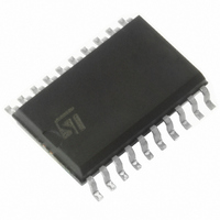
IC MOSFET DRVR TRPL HI SIDE SO20
Manufacturer
STMicroelectronics
Type
Triple High-Side Mosfet Driverr
Datasheet
1.L9380-TR.pdf
(18 pages)
Specifications of L9380
Configuration
High-Side
Input Type
Non-Inverting
Current - Peak
3mA
Number Of Configurations
3
Number Of Outputs
3
Voltage - Supply
7 V ~ 18.5 V
Operating Temperature
-40°C ~ 150°C
Mounting Type
Surface Mount
Package / Case
20-SOIC (7.5mm Width)
Supply Current
2.5 mA
Maximum Operating Temperature
+ 150 C
Mounting Style
SMD/SMT
Minimum Operating Temperature
- 40 C
Number Of Drivers
3
Lead Free Status / RoHS Status
Lead free / RoHS Compliant
Delay Time
-
High Side Voltage - Max (bootstrap)
-
Lead Free Status / Rohs Status
Lead free / RoHS Compliant
Available stocks
Company
Part Number
Manufacturer
Quantity
Price
Part Number:
L9380
Manufacturer:
ST
Quantity:
20 000
L9380
Functional description
Figure 5.
Comparator hysteresis
V
T
D98AT394
-10mV
+10mV
V
V
Dr
So
The application diagram is shown in
Figure
6. Because of the transients present at the
power lines during operation and possible disturbances in the system the external resistors
are necessary.
Positive ISO-Pulses at Drain, Gate Source are clamped with an active clamping structure.
The clamping voltage is less than 60V. Negative Pulses are only clamped with the ESD-
Structure less than -15 V. This transients lower than -15 V can influence the other channels.
In order to protect the transistor against overload and gate breakdown protection diodes
between gate and source and gate and drain has to be connected. In case of overvoltage
into V
(V
> 20 V) the charge pump oscillation is stopped.
S
S
Then the charge pump capacitor will be loaded by a diode and a resistor in series up to V
S
(see
Figure
1). In this case the channels are not influenced. In reverse battery condition the
pins D1, D2, S1, S2 follow the battery potential down to -13 V (high impedance) and the
gate driver pins G1, G2 is referred to S1, S2. In this way it is assured that M1 and M2 will not
be driven into the linear conductive mode. This protection function is operating for V
, V
S1
S2
down to -15 V. The gate driver output G3 is referred to the D1 in this case. This function
guarantees that the source to source connected N-Channel MOS transistors M3 and M4
remains OFF.
All the supplies and the in- and output of the PC Board are supplied with a 40 wires flat
cable (not used wires are left open). This cable is submitted to the RF in the strip-line like
described in DIN 40839-4 or ISO 11456-5.
The measured circuit was build up on a PCB board with ground plane. In the frequency
range from 1 MHz to 400 MHz and 80 % AM-modulation of 1 kHz with field strength of
200 V/m no influence to the basic function was detected on a typical device.
The failure criteria is an envelope of the output signal with 20 % in the amplitude and 2 % in
the time.
Doc ID 5853 Rev 3
11/18


