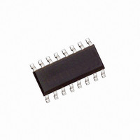
HCPL-316J Avago Technologies US Inc., HCPL-316J Datasheet - Page 28

HCPL-316J
Manufacturer Part Number
HCPL-316J
Description
OPTOCOUPLER GATE DRV 2A 16-SOIC
Manufacturer
Avago Technologies US Inc.
Datasheet
1.HCPL-316J-500E.pdf
(33 pages)
Specifications of HCPL-316J
Configuration
High-Side
Input Type
Differential
Delay Time
300ns
Current - Peak
2.5A
Number Of Configurations
1
Number Of Outputs
1
Voltage - Supply
4.5 V ~ 5.5 V
Operating Temperature
-40°C ~ 100°C
Mounting Type
Surface Mount
Package / Case
16-SOIC (0.300", 7.5mm Width)
No. Of Channels
1
Isolation Voltage
3.75kV
Optocoupler Output Type
Gate Drive
Input Current
22mA
Output Voltage
30V
Opto Case Style
SOIC
No. Of Pins
16
Propagation Delay Low-high
0.5µs
Lead Free Status / RoHS Status
Contains lead / RoHS non-compliant
High Side Voltage - Max (bootstrap)
-
Lead Free Status / RoHS Status
Contains lead / RoHS non-compliant, Contains lead / RoHS non-compliant
Other names
516-1130-5
Available stocks
Company
Part Number
Manufacturer
Quantity
Price
Company:
Part Number:
HCPL-316J
Manufacturer:
AVAGO
Quantity:
20 700
Company:
Part Number:
HCPL-316J
Manufacturer:
AD
Quantity:
1 939
Part Number:
HCPL-316J
Manufacturer:
AGILENT
Quantity:
20 000
Company:
Part Number:
HCPL-316J#500
Manufacturer:
AGILENT
Quantity:
3 169
Part Number:
HCPL-316J#500
Manufacturer:
AGILENT
Quantity:
20 000
Company:
Part Number:
HCPL-316J-000E
Manufacturer:
KOITECH
Quantity:
713
Company:
Part Number:
HCPL-316J-000E
Manufacturer:
AVAGO
Quantity:
21 000
Part Number:
HCPL-316J-000E
Manufacturer:
AVAGO/安华高
Quantity:
20 000
Part Number:
HCPL-316J-500E
Manufacturer:
AVAGO/安华高
Quantity:
20 000
Part Number:
HCPL-316J-500E/HCPL316J-500E
Manufacturer:
AVAGO/安华高
Quantity:
20 000
User-Configuration of the HCPL-316J Output Side R
and Optional Resistor R
The value of the gate resistor R
determines the maximum amount of gate-charging/dis-
charging current (I
be carefully chosen to match the size of the IGBT being
driven. Often it is desirable to have the peak gate charge
current be somewhat less than the peak discharge cur-
rent (I
resistor (R
determine I
diode. As an example, refer to Figure 74. Assuming that
R
Figure 74. Use of R
Figure 73c. Safe hardware reset for inverting input configuration.
28
G
HCPL-316J
is already determined and that the design I
μC
ON,PEAK
RESET
FAULT
V
IN-
C
V
DESAT
) can be used along with R
LED2+
ON,PEAK
V
V
OUT
CC2
V
V
V
V
< I
EE
EE
C
C
E
to further limit I
OFF,PEAK
16
15
14
13
12
11
10
9
ON,PEAK
V
V
and I
CC
CC
10 Ω
10 nF
OFF,PEAK
R
C
). For this condition, an optional
1
2
3
4
5
6
7
8
100 pF
C
15 V
:
and I
8 Ω
ON,PEAK
V
V
V
GND1
RESET
FAULT
V
V
IN+
IN-
CC1
LED1+
LED1-
G
OFF,PEAK
(along with V
without using a steering
.
HCPL-316J
-5 V
G
) and thus should
to independently
CC2
OH,PEAK
and V
G
EE
=
)
Figure 73d. Safe hardware reset for inverting input configuration
(automatically resets for every V
0.5 A, the value of R
way:
R
See “Power and Layout Considerations” section for more
information on calculating value of R
C
+ R
μC
R
G
C
= [4 V – (-5 V)]
= 18 Ω
= [V
V
FAULT
= 8 Ω
IN-
RESET
CC2
0.5 A
I
OH,PEAK
– V
OH
V
V
CC
CC
C
– (V
can be estimated in the following
1
2
3
4
5
6
7
8
IN-
EE
input).
)]
V
V
V
GND1
RESET
FAULT
V
V
IN+
IN-
CC1
LED1+
LED1-
HCPL-316J
G
.


