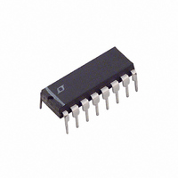
LT1336IN Linear Technology, LT1336IN Datasheet - Page 4

LT1336IN
Manufacturer Part Number
LT1336IN
Description
IC MOSFET DRVR 1/2BRDG NCH 16DIP
Manufacturer
Linear Technology
Datasheet
1.LT1336CSPBF.pdf
(20 pages)
Specifications of LT1336IN
Configuration
Half Bridge
Input Type
Differential
Delay Time
250ns
Current - Peak
1.5A
Number Of Configurations
1
Number Of Outputs
2
High Side Voltage - Max (bootstrap)
60V
Voltage - Supply
10 V ~ 15 V
Operating Temperature
-40°C ~ 85°C
Mounting Type
Through Hole
Package / Case
16-DIP (0.300", 7.62mm)
Lead Free Status / RoHS Status
Contains lead / RoHS non-compliant
Available stocks
Company
Part Number
Manufacturer
Quantity
Price
Part Number:
LT1336IN#PBF
Manufacturer:
LINEAR/凌特
Quantity:
20 000
LT1336
elecTrical characTerisTics
Note 1: Stresses beyond those listed under Absolute Maximum Ratings
may cause permanent damage to the device. Exposure to any Absolute
Maximum Rating condition for extended periods may affect device
reliability and lifetime.
Note 2: T
dissipation P
Typical perForMance characTerisTics
temperature range, otherwise specifications are at T
Feedback pins connected to Gate Drive pins unless otherwise specified.
SYMBOL PARAMETER
t
t
4
D3
D4
LT1336CN/LT1336IN: T
LT1336CS/LT1336IS: T
22
20
18
16
14
12
10
8
6
4
DC Supply Current
vs Supply Voltage
J
is calculated from the ambient temperature T
V
Top Gate Lockout Delay
Bottom Gate Lockout Delay
Top Gate Release Delay
Bottom Gate Release Delay
INBOTTOM
D
6
V
according to the following formulas:
INTOP
8
SUPPLY VOLTAGE (V)
= HIGH
= LOW
10
J
J
12
= T
= T
HIGH OR LOW
BOTH INPUTS
A
A
V
V
14
+ (P
INTOP
INBOTTOM
+ (P
V
TSOURCE
D
D
16
= LOW
)(110°C/W)
)(70°C/W)
= HIGH
= 0V
18
1336 G01
20
A
and power
18
17
16
15
14
13
12
11
10
CONDITIONS
V
Measured at V
V
Measured at V
V
Measured at V
V
Measured at V
9
–50
INBOTTOM
INTOP
INBOTTOM
INTOP
A
DC Supply Current
vs Temperature
= 25°C. Test Circuit, V
V
INBOTTOM
–25
(+) Transition, V
(–) Transition, V
V
INTOP
The
(+) Transition, V
(–) Transition, V
V
0
= HIGH
= LOW
l
TEMPERATURE (C)
TGATE DR
BGATE DR
TGATE DR
BGATE DR
INBOTTOM
denotes the specifications which apply over the full operating
V
BOTH INPUTS
HIGH OR LOW
INTOP
25
Note 3: Dynamic supply current is higher due to the gate charge
being delivered at the switching frequency. See Typical Performance
Characteristics and Applications Information sections.
Note 4: Pins 1 and 16 connected to each end of the inductor. Booster is
free running.
Note 5: See Timing Diagram. Gate rise times are measured from 2V to 10V
and fall times are measured from 10V to 2V. Delay times are measured
from the input transition to when the gate voltage has risen to 2V or
decreased to 10V.
INBOTTOM
INBOTTOM
= HIGH
– V
– V
(Note 5)
(Note 5)
= LOW
50
TSOURCE
TSOURCE
INTOP
INTOP
V
V
TSOURCE
+
+
75
= 12V
= V
= 2V,
= 2V,
= 2V,
= 2V,
100
BOOST
(Note 5)
(Note 5)
= 0V
1336 G02
125
= 12V, V
TSOURCE
34
31
28
25
22
19
16
13
10
l
l
l
l
0
DC Supply Current
vs Top Source Voltage
V
+
= 12V
5
MIN
= 0V and Pins 1, 16 open. Gate
TOP SOURCE VOLTAGE (V)
HIGH OR LOW
BOTH INPUTS
10
V
INBOTTOM
V
15
INTOP
TYP
300
250
250
200
V
V
INTOP
INBOTTOM
= HIGH
20
= LOW
= HIGH
25
MAX
600
500
500
400
= LOW
30
35
1336 G18
UNITS
1336fa
40
ns
ns
ns
ns


