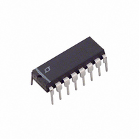
LT1336IN Linear Technology, LT1336IN Datasheet - Page 13

LT1336IN
Manufacturer Part Number
LT1336IN
Description
IC MOSFET DRVR 1/2BRDG NCH 16DIP
Manufacturer
Linear Technology
Datasheet
1.LT1336CSPBF.pdf
(20 pages)
Specifications of LT1336IN
Configuration
Half Bridge
Input Type
Differential
Delay Time
250ns
Current - Peak
1.5A
Number Of Configurations
1
Number Of Outputs
2
High Side Voltage - Max (bootstrap)
60V
Voltage - Supply
10 V ~ 15 V
Operating Temperature
-40°C ~ 85°C
Mounting Type
Through Hole
Package / Case
16-DIP (0.300", 7.62mm)
Lead Free Status / RoHS Status
Contains lead / RoHS non-compliant
Available stocks
Company
Part Number
Manufacturer
Quantity
Price
Part Number:
LT1336IN#PBF
Manufacturer:
LINEAR/凌特
Quantity:
20 000
applicaTions inForMaTion
Paralleling MOSFETs
When the above calculations result in a lower R
than is economically feasible with a single MOSFET, two
or more MOSFETs can be paralleled. The MOSFETs will
inherently share the currents according to their R
ratio as long as they are thermally connected (e.g., on a
common heat sink). The LT1336 top and bottom drivers
can each drive five power MOSFETs in parallel with only a
small loss in switching speeds (see Typical Performance
Characteristics). A low value resistor (10Ω to 47Ω) in
series with each individual MOSFET gate may be required
to “decouple” each MOSFET from its neighbors to pre-
vent high frequency oscillations (consult manufacturer’s
recommendations). If gate decoupling resistors are used,
the corresponding Gate Feedback pin can be connected
to any one of the gates as shown in Figure 3.
Driving multiple MOSFETs in parallel may restrict the
operating frequency to prevent overdissipation in the
LT1336 (see the following Gate Charge and Driver
Dissipation).
Gate Charge and Driver Dissipation
A useful indicator of the load presented to the driver by
a power MOSFET is the total gate charge Q
cludes the additional charge required by the gate-to-drain
swing. Q
0.8V
switching application, it will be larger than given by the DC
electrical characteristics because of the additional supply
current associated with sourcing the MOSFET gate charge:
I
SUPPLY
DS(MAX)
*OPTIONAL 10
G
is usually specified for V
=I
LT1336
. When the supply current is measured in a
GATEDR
DC
GATEFB
Figure 3. Paralleling MOSFETs
+
dQ
dt
G
R
G
*
TOP
+
dQ
dt
R
GS
G
G
*
= 10V and V
BOTTOM
G
HV
1336 F03
, which in-
+
DS(ON)
DS(ON)
DS
=
The actual increase in supply current is slightly higher
due to LT1336 switching losses and the fact that the gates
are being charged to more than 10V. Supply Current vs
Switching Frequency is given in the Typical Performance
Characteristics.
The LT1336 junction temperature can be estimated by
using the equations given in Note 1 of the Electrical Char-
acteristics. For example, the LT1336IS is limited to less
than 31mA from a 12V supply:
In order to prevent the maximum junction temperature
from being exceeded, the LT1336 supply current must be
verified while driving the full complement of the chosen
MOSFET type at the maximum switching frequency.
Ugly Transient Issues
In PWM applications the drain current of the top MOSFET
is a square wave at the input frequency and duty cycle. To
prevent large voltage transients at the top drain, a low ESR
electrolytic capacitor must be used and returned to the
power ground. The capacitor is generally in the range of
25µF to 5000µF and must be physically sized for the RMS
current flowing in the drain to prevent heating and prema-
ture failure. In addition, the LT1336 requires a separate
10µF capacitor connected closely between Pins 2 and 6.
The LT1336 top source is internally protected against
transients below ground and above supply. However, the
Gate Drive pins cannot be forced below ground. In most
applications, negative transients coupled from the source
to the gate of the top MOSFET do not cause any problems.
Switching Regulator Applications
The LT1336 is ideal as a synchronous switch driver to
improve the efficiency of step-down (buck) switching
regulators. Most step-down regulators use a high current
Schottky diode to conduct the inductor current when the
switch is off. The fractions of the oscillator period that the
switch is on (switch conducting) and off (diode conduct-
ing) are given by:
T
J
= 85°C + (31mA)(12V)(110°C/W)
= 126°C exceeds absolute maximum
LT1336
13
1336fa


