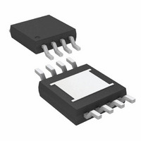
LTC4444EMS8E-5#TRPBF Linear Technology, LTC4444EMS8E-5#TRPBF Datasheet - Page 6

LTC4444EMS8E-5#TRPBF
Manufacturer Part Number
LTC4444EMS8E-5#TRPBF
Description
IC MOSFET DRIVER N-CH 8-MSOP
Manufacturer
Linear Technology
Datasheet
1.LTC4444IMS8E-5PBF.pdf
(14 pages)
Specifications of LTC4444EMS8E-5#TRPBF
Configuration
High and Low Side, Synchronous
Input Type
Differential, PWM
Delay Time
33ns
Current - Peak
1.4A
Number Of Configurations
1
Number Of Outputs
2
High Side Voltage - Max (bootstrap)
114V
Voltage - Supply
4.5 V ~ 13.5 V
Operating Temperature
-40°C ~ 85°C
Mounting Type
Surface Mount
Package / Case
8-MSOP Exposed Pad, 8-HMSOP, 8-eMSOP
Lead Free Status / RoHS Status
Lead free / RoHS Compliant
Available stocks
Company
Part Number
Manufacturer
Quantity
Price
LTC4444-5
PIN FUNCTIONS
TINP (Pin 1): High Side Input Signal. Input referenced
to GND. This input controls the high side driver output
(TG).
BINP (Pin 2): Low Side Input Signal. This input controls
the low side driver output (BG).
V
and the low side gate driver output directly and the high
side gate driver output through an external diode con-
nected between this pin and BOOST (Pin 6). A low ESR
ceramic bypass capacitor should be tied between this pin
and GND (Pin 9).
BG (Pin 4): Low Side Gate Driver Output (Bottom Gate).
This pin swings between V
NC (Pin 5): No Connect. No connection required.
TYPICAL PERFORMANCE CHARACTERISTICS
6
CC
(Pin 3): Supply. This pin powers input buffers, logic
1.8
1.4
1.2
1.0
0.8
0.4
1.6
0.6
0.2
0
0
Switching Supply Current
vs Input Frequency
T
V
TS = GND
A
CC
= 25°C
(TG SWITCHING)
= BOOST = 6V
200
SWITCHING FREQUENCY (kHz)
CC
I
I
VCC
BOOST
I
BOOST
and GND.
400
(TG SWITCHING)
(BG SWITCHING)
600
I
(BG SWITCHING)
VCC
800
44445 G18
1000
BOOST (Pin 6): High Side Bootstrapped Supply. An ex-
ternal capacitor should be tied between this pin and TS
(Pin 8). Normally, a bootstrap diode is connected between
V
V
age drop of the bootstrap diode.
TG (Pin 7): High Side Gate Driver Output (Top Gate). This
pin swings between TS and BOOST.
TS (Pin 8): High Side MOSFET Source Connection (Top
Source).
GND (Exposed Pad Pin 9): Ground. Must be soldered to
PCB ground for optimal thermal performance.
CC
CC
1000
100
(Pin 3) and this pin. Voltage swing at this pin is from
– V
10
1
0
1
D
Switching Supply Current
vs Load Capacitance
(TG SWITCHING AT 1MHz)
I
(TG SWITCHING AT 500kHz)
(BG SWITCHING
BOOST
to V
AT 1MHz)
2
I
(BG SWITCHING AT 500kHz)
VCC
IN
3
I
LOAD CAPACITANCE (nF)
BOOST
I
+ V
VCC
4
CC
5
– V
(BG SWITCHING
6
AT 500kHz)
D
I
(TG SWITCHING
(TG SWITCHING
, where V
VCC
7
AT 1MHz)
AT 1MHz)
I
BOOST
I
8
VCC
9
44445 G19
D
10
is the forward volt-
44445fc


