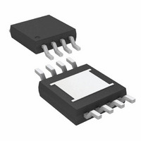
LTC4444EMS8E-5#TRPBF Linear Technology, LTC4444EMS8E-5#TRPBF Datasheet

LTC4444EMS8E-5#TRPBF
Specifications of LTC4444EMS8E-5#TRPBF
Available stocks
Related parts for LTC4444EMS8E-5#TRPBF
LTC4444EMS8E-5#TRPBF Summary of contents
Page 1
... Automotive Power Supplies n High Density Power Modules n Telecommunication Systems L, LT, LTC, LTM, Linear Technology and the Linear logo are registered trademarks and trademark of Linear Technology Corporation. All other trademarks are the SENSE property of their respective owners. Protected by U.S. Patents, including 6677210. ...
Page 2
... Storage Temperature Range ..................–65°C to 150°C Lead Temperature (Soldering, 10 sec) ................... 300°C ORDER INFORMATION LEAD FREE FINISH TAPE AND REEL LTC4444EMS8E-5#PBF LTC4444EMS8E-5#TRPBF LTC4444IMS8E-5#PBF LTC4444IMS8E-5#TRPBF LTC4444HMS8E-5#PBF LTC4444HMS8E-5#TRPBF LTC4444MPMS8E-5#PBF LTC4444MPMS8E-5#TRPBF Consult LTC Marketing for parts specified with wider operating temperature ranges. *The temperature grade is identified by a label on the shipping container. ...
Page 3
ELECTRICAL CHARACTERISTICS temperature range, otherwise specifications are at T SYMBOL PARAMETER I Input Pin Bias Current TINP(BINP) High Side Gate Driver Output (TG High Output Voltage OH(TG Low Output Voltage OL(TG Peak Pull-Up Current ...
Page 4
LTC4444-5 TYPICAL PERFORMANCE CHARACTERISTICS V Supply Quiescent Current CC vs Voltage 450 T = 25°C A BOOST = 6V 400 TINP = BINP = GND 350 300 TINP (BINP 250 200 150 100 50 0 ...
Page 5
TYPICAL PERFORMANCE CHARACTERISTICS Input Thresholds (TINP , BINP) Hysteresis vs Temperature 500 V = BOOST = GND 475 450 425 400 375 –55 – 125 150 TEMPERATURE (°C) 44445 G10 Rise and ...
Page 6
LTC4444-5 TYPICAL PERFORMANCE CHARACTERISTICS Switching Supply Current vs Input Frequency 1 25° BOOST = 6V 1 GND 1.4 1.2 I BOOST (TG SWITCHING) 1.0 0.8 0.6 I (TG SWITCHING) VCC 0.4 I ...
Page 7
BLOCK DIAGRAM 4.5V TO 13.5V GND 9 TINP 1 BINP 2 TIMING DIAGRAMS BINP BG TINP TG-TS TINP (BINP) BINP (TINP) BG (TG) TG (BG) UVLO CC HIGH SIDE LEVEL SHIFTER LDO V INT ANTISHOOT-THROUGH PROTECTION ...
Page 8
LTC4444-5 OPERATION Overview The LTC4444-5 receives ground-referenced, low voltage digital input signals to drive two N-channel power MOSFETs in a synchronous buck power supply configuration. The gate of the low side MOSFET is driven either to V depending on the ...
Page 9
OPERATION pull-down on the driver outputs is the prevention of cross- conduction current. For example, when BG turns the low side (synchronous) power MOSFET off and TG turns the high side power MOSFET on, the voltage on the TS pin ...
Page 10
LTC4444-5 APPLICATIONS INFORMATION At a particular switching frequency, the internal power loss increases due to both AC currents required to charge and discharge internal node capacitances and cross-conduc- tion currents in the internal logic gates. The sum of the quiescent ...
Page 11
TYPICAL APPLICATION LTC3780 High Efficiency 36V to 72V V 10k 0.022μF 100Ω SENSE PGOOD 1000pF 2 220k 68pF SS 100Ω 3 – SENSE SENSE 100pF 4 SENSE 0.1μF 5 487k + V I 100V ...
Page 12
LTC4444-5 PACKAGE DESCRIPTION 1.88 0.102 (.074 .004) 5.23 (.206) MIN 0.42 0.038 (.0165 .0015) TYP RECOMMENDED SOLDER PAD LAYOUT DETAIL “A” 0.254 (.010) GAUGE PLANE DETAIL “A” 0.18 (.007) NOTE: 1. DIMENSIONS IN MILLIMETER/(INCH) 2. DRAWING NOT TO SCALE 3. ...
Page 13
... H-grade part added. Reflected throughout the data sheet. Information furnished by Linear Technology Corporation is believed to be accurate and reliable. However, no responsibility is assumed for its use. Linear Technology Corporation makes no representa- tion that the interconnection of its circuits as described herein will not infringe on existing patent rights. ...
Page 14
... Peak Pull-Up/ CC ≤ 15V, 2.4A Peak Pull-Up/ CC ≤ 9.5V, 3.2A Peak Pull-Up/ CC ≤ 6.5V, 3.2A Peak Pull-Up/ CC ≤ 25V, 6A Peak Output Current CC LT 0111 REV C • PRINTED IN USA © LINEAR TECHNOLOGY CORPORATION 2008 100μF 80V 100V 2 V OUT 12V ...


