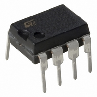
L6387E STMicroelectronics, L6387E Datasheet - Page 7

L6387E
Manufacturer Part Number
L6387E
Description
IC DRIVER HI/LO SIDE HV 8-DIP
Manufacturer
STMicroelectronics
Type
High Side/Low Sider
Datasheet
1.L6387ED013TR.pdf
(15 pages)
Specifications of L6387E
Configuration
High and Low Side, Independent
Input Type
Non-Inverting
Delay Time
110ns
Current - Peak
400mA
Number Of Configurations
1
Number Of Outputs
2
High Side Voltage - Max (bootstrap)
600V
Voltage - Supply
17V
Operating Temperature
-40°C ~ 125°C
Mounting Type
Through Hole
Package / Case
8-DIP (0.300", 7.62mm)
Product
Half-Bridge Drivers
Rise Time
50 ns
Fall Time
30 ns
Maximum Power Dissipation
750 mW
Maximum Operating Temperature
+ 125 C
Mounting Style
Through Hole
Maximum Turn-off Delay Time
105 ns
Maximum Turn-on Delay Time
110 ns
Minimum Operating Temperature
- 45 C
Number Of Drivers
2
Lead Free Status / RoHS Status
Lead free / RoHS Compliant
Other names
497-6217-5
Available stocks
Company
Part Number
Manufacturer
Quantity
Price
Part Number:
L6387ED
Manufacturer:
ST
Quantity:
20 000
Company:
Part Number:
L6387ED013TR
Manufacturer:
st
Quantity:
1 156
Part Number:
L6387ED013TR
Manufacturer:
ST
Quantity:
20 000
L6387E
5
5.1
Bootstrap driver
A bootstrap circuitry is needed to supply the high voltage section. This function is normally
accomplished by a high voltage fast recovery diode
integrated structure replaces the external diode. It is realized by a high voltage DMOS,
driven synchronously with the low side driver (LVG), with in series a diode, as shown in
Figure 3
diode connected in series to the DMOS has been added to avoid undesirable turn on of it.
C
To choose the proper C
capacitor. This capacitor C
The ratio between the capacitors C
It has to be:
e.g.: if Q
300mV.
If HVG has to be supplied for a long time, the C
the leakage losses.
e.g.: HVG steady state consumption is lower than 200µA, so if HVG T
to supply 1µC to C
The internal bootstrap driver gives great advantages: the external fast recovery diode can
be avoided (it usually has great leakage current).
This structure can work only if V
LVG is on. The charging time (T
fulfilled and it has to be long enough to charge the capacitor.
The bootstrap driver introduces a voltage drop due to the DMOS R
Ω). At low frequency this drop can be neglected. Anyway increasing the frequency it must be
taken in to account.
The following equation is useful to compute the drop on the bootstrap DMOS:
where Q
bootstrap DMOS, and T
BOOT
gate
gate
b. An internal charge pump
selection and charging
is 30nC and V
is the gate charge of the external power MOS, R
EXT
. This charge on a 1µF capacitor means a voltage drop of 1V.
BOOT
charge
V
drop
EXT
gate
value the external MOS can be seen as an equivalent
is the charging time of the bootstrap capacitor.
=
is related to the MOS total gate charge:
is 10V, C
charge
OUT
I
ch
EXT
arg
is close to GND (or lower) and in the meanwhile the
(Figure 3
) of the C
e
and C
R
C
EXT
C
dson
EXT
BOOT
is 3nF. With C
BOOT
→
>>>C
=
b) provides the DMOS driving voltage. The
V
BOOT
Q
-------------- -
V
BOOT
drop
gate
gate
EXT
is proportional to the cyclical voltage loss.
(Figure 3
is the time in which both conditions are
=
selection has to take into account also
------------------ - R
T
Q
ch
gate
BOOT
arg
e
dson
a). In the L6387E a patented
= 100nF the drop would be
dson
is the on resistance of the
DSON
ON
(typical value: 125
is 5ms, C
Bootstrap driver
BOOT
has
7/15


