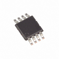
MAX1614EUA+ Maxim Integrated Products, MAX1614EUA+ Datasheet - Page 5

MAX1614EUA+
Manufacturer Part Number
MAX1614EUA+
Description
IC DVR MOSFET HI-SIDE NCH 8-UMAX
Manufacturer
Maxim Integrated Products
Type
High Side Driverr
Datasheet
1.MAX1614EUA.pdf
(8 pages)
Specifications of MAX1614EUA+
Configuration
High-Side
Input Type
Non-Inverting
Number Of Configurations
1
Number Of Outputs
1
Voltage - Supply
5 V ~ 26 V
Operating Temperature
-40°C ~ 85°C
Mounting Type
Surface Mount
Package / Case
8-MSOP, Micro8™, 8-uMAX, 8-uSOP,
Product
Driver ICs - Various
Supply Voltage (max)
26 V
Supply Voltage (min)
5 V
Supply Current
21 uA
Maximum Power Dissipation
330 mW
Maximum Operating Temperature
+ 85 C
Mounting Style
SMD/SMT
Minimum Operating Temperature
- 40 C
Number Of Drivers
1
Output Current
60 uA
Lead Free Status / RoHS Status
Lead free / RoHS Compliant
Delay Time
-
Current - Peak
-
High Side Voltage - Max (bootstrap)
-
Lead Free Status / Rohs Status
Lead free / RoHS Compliant
The MAX1614 uses an internal, monolithic charge pump
and low-dropout linear regulator to supply the required
8V V
high-side switch (Figure 1). The charge pump typically
supplies 30µA, charging 800pF of gate capacitance in
400µs (V
add a small capacitor between the GATE and SRC
pins. When turned off, GATE and SRC pull low and typi-
cally discharge an 800pF gate capacitance in 80µs.
The MAX1614 provides separate on/off control inputs
(ON and OFF). ON and OFF connect, respectively, to
the SET and RESET inputs of an internal flip-flop. When
ON is pulsed low (with OFF = high), the internal charge
pump turns on, and GATE is pumped to 8V above SRC,
turning on the external MOSFETs. The charge pump
maintains gate drive to the external MOSFETs until OFF
is pulsed low. When this happens, the internal charge
pump turns off, and GATE discharges to ground
through an internal switch. For slower turn-on times,
simply add a small capacitor.
__________ Applications Information
ON and OFF internally connect to 2µA max pull-up
current sources (Figure 1). The open-circuit voltage
for ON and OFF ranges from 7V to 10.5V (nominally
8.5V). Since the current sources are relatively weak,
connecting ON and OFF directly to logic powered from
_______________Detailed Description
______________________________________________________________Pin Description
PIN
1
2
3
4
5
6
7
8
GS
Connecting ON / OFF to 3V or 5V Logic
voltage to fully enhance an N-channel MOSFET
BATT
NAME
GATE
BATT
GND
LBO
SRC
OFF
ON
LBI
= 15V). For slower turn-on times, simply
_______________________________________________________________________________________
SET Input to the On/Off Latch. Pulse ON low with OFF high to turn on the external MOSFET switch. When
both ON and OFF are low, the part is off.
RESET Input to the On/Off Latch. Pulse OFF low with ON high to turn off the external MOSFET switch. When
both ON and OFF are low, the part is off.
Open-Drain, Low-Battery Comparator Output. LBO is low when V
Low-Battery Comparator Input. LBO goes low when V
between BATT, LBI, and GND to set the battery undervoltage trip threshold (see Typical Operating Circuit ).
System Ground
Gate-Drive Output. Connect to the gates of external, N-channel MOSFETs. When the MAX1614 is off, GATE
actively pulls to GND.
Source Input. Connect to the sources of external, N-channel MOSFETs. When the MAX1614 is off, SRC
actively pulls to GND.
Battery Input. Connect to a battery voltage between 5V and 26V.
High-Side, N-Channel MOSFET
lower voltages (e.g., 3V or 5V) poses no problem if the
gate outputs driving these pins can sink at least 2µA
while high.
Although the MAX1614 shutdown function was designed
to operate with a single pushbutton on/off switch, it can
also be driven by a single gate. Connect ON to GND
and drive OFF directly (Figure 2).
The MAX1614 is not intended for fast switching appli-
cations. In fact, it is specifically designed to limit the
rate of change of the load current, I/ t. The maximum
switching rate is limited by the turn-on time, which is a
function of the charge-pump output current and the
total capacitance on GATE (C
on time as a function of external MOSFET gate capaci-
tance using the Gate Charging Current vs. V
in the Typical Operating Characteristics . Since turn-off
time is small compared to turn-on time, the maximum
switching rate is approximately 1/t
The charge pump uses an internal monolithic transfer
capacitor to charge the external MOSFET gates.
Normally, the external MOSFET’s gate capacitance is
sufficient to serve as a reservoir capacitor. If the
MOSFETs are located at a significant distance from the
MAX1614, place a local bypass capacitor (100pF typ)
across the GATE and SRC pins. For slower turn-on
times, simply add a small capacitor between GATE and
SRC.
FUNCTION
LBI
falls below 1.20V (typ). Connect a voltage divider
LBI
is below the trip point.
Maximum Switching Rate
Adding Gate Capacitance
Switch Driver
GATE
ON
). Calculate the turn-
.
BATT
graph
5


