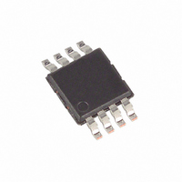
MAX1614EUA+ Maxim Integrated Products, MAX1614EUA+ Datasheet - Page 2

MAX1614EUA+
Manufacturer Part Number
MAX1614EUA+
Description
IC DVR MOSFET HI-SIDE NCH 8-UMAX
Manufacturer
Maxim Integrated Products
Type
High Side Driverr
Datasheet
1.MAX1614EUA.pdf
(8 pages)
Specifications of MAX1614EUA+
Configuration
High-Side
Input Type
Non-Inverting
Number Of Configurations
1
Number Of Outputs
1
Voltage - Supply
5 V ~ 26 V
Operating Temperature
-40°C ~ 85°C
Mounting Type
Surface Mount
Package / Case
8-MSOP, Micro8™, 8-uMAX, 8-uSOP,
Product
Driver ICs - Various
Supply Voltage (max)
26 V
Supply Voltage (min)
5 V
Supply Current
21 uA
Maximum Power Dissipation
330 mW
Maximum Operating Temperature
+ 85 C
Mounting Style
SMD/SMT
Minimum Operating Temperature
- 40 C
Number Of Drivers
1
Output Current
60 uA
Lead Free Status / RoHS Status
Lead free / RoHS Compliant
Delay Time
-
Current - Peak
-
High Side Voltage - Max (bootstrap)
-
Lead Free Status / Rohs Status
Lead free / RoHS Compliant
ABSOLUTE MAXIMUM RATINGS
BATT, SRC to GND.................................................-0.3V to +30V
GATE to SRC ..........................................................-0.3V to +12V
GATE to GND .........................................................-0.3V to +36V
GATE + SRC Sink Current, Continuous .............................2.7mA
LBI, LBO, ON, OFF to GND....................................-0.3V to +12V
LBO Current ..........................................................................5mA
High-Side, N-Channel MOSFET
Switch Driver
ELECTRICAL CHARACTERISTICS
(V
Stresses beyond those listed under “Absolute Maximum Ratings” may cause permanent damage to the device. These are stress ratings only, and functional
operation of the device at these or any other conditions beyond those indicated in the operational sections of the specifications is not implied. Exposure to
absolute maximum rating conditions for extended periods may affect device reliability.
2
BATT Operating Range
BATT Shutdown Current
Quiescent Current
INTERNAL CHARGE PUMP
GATE Drive Voltage
GATE Drive Output Current
GATE Discharge Current
LOW-BATTERY COMPARATOR
LBI Trip Level
LBI Trip Hysteresis
Minimum V
LBI Input Current
LBO Low Voltage
LBO High Leakage
CONTROL INPUTS (
Minimum Input Pull-Up Current
Maximum Input Pull-Up Current
Input Low Voltage
Input High Voltage
Minimum Input Pulse Width
BATT
_______________________________________________________________________________________
= 15V, T
PARAMETER
BATT
A
for Valid LBO
= 0°C to +85°C, unless otherwise noted. Typical values are at T
ON
,
OFF
)
SYMBOL
I
I
BATT
SHDN
I
V
V
V
V
I
V
t
SRC
V
LBI
PW
OH
GS
TH
OL
IH
IL
+
V
I
V
I
SRC = BATT
V
V
I
SRC = BATT
Measured from GATE to SRC, V
I
Measured from GATE to SRC, V
I
V
V
LBI input falling
Tested at V
V
I
V
Tested at 2V
Tested at 0.6V
V
V
V
GATE
GATE
GATE
GATE
GATE
SINK
BATT
BATT
GATE
BATT
GATE
GATE
LBI
LBO
BATT
BATT
BATT
= 1.3V
= 1mA
= 11.5V
= 0A, device latched off, V
= 0A, device latched on, V
= 1.5µA
= 15V, ON = OFF = unconnected,
= 0A, device latched on, V
= 0A
= 26V, ON = OFF = unconnected,
= 26V, ON = OFF = unconnected,
= 5V
= 26V
= 5V
- V
= V
= 4V, device latched off
SRC
SRC
LBI
> 3V, SRC = BATT
= V
= 15V
CONDITIONS
BATT
Continuous Power Dissipation (T
Operating Temperature Range ...........................-40°C to +85°C
Junction Temperature ......................................................+150°C
Storage Temperature Range .............................-65°C to +160°C
Lead Temperature (soldering, 10sec) .............................+300°C
/ 4
µMAX (derate 4.10mV/°C above +70°C) .....................330mW
BATT
BATT
LBI
LBI
LBI
A
= V
= 1.5V
= 1.5V,
= 1.5V,
= 15V,
= +25°C.)
SRC
= 5V,
1.182
MIN
6.5
0.5
0.5
2.0
15
5
3
A
= +70°C)
0.02V
TYP
1.20
0.9
1.5
0.5
17
21
4
8
TH
1.218
MAX
9.0
0.4
0.5
0.6
1.0
26
30
40
60
10
7
2
4
2
UNITS
mA
µA
µA
µA
µA
nA
µA
µA
µA
µs
V
V
V
V
V
V
V
V


