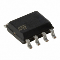
L6384D013TR STMicroelectronics, L6384D013TR Datasheet - Page 2

L6384D013TR
Manufacturer Part Number
L6384D013TR
Description
IC DRIVER HALF BRIDGE HV 8SOIC
Manufacturer
STMicroelectronics
Type
Driverr
Datasheet
1.L6384D013TR.pdf
(10 pages)
Specifications of L6384D013TR
Configuration
Half Bridge
Input Type
Inverting
Current - Peak
400mA
Number Of Configurations
1
Number Of Outputs
2
High Side Voltage - Max (bootstrap)
600V
Voltage - Supply
8 V ~ 16.6 V
Operating Temperature
-45°C ~ 125°C
Mounting Type
Surface Mount
Package / Case
8-SOIC (3.9mm Width)
Rise Time
70 ns
Fall Time
30 ns
Supply Voltage (min)
8 V
Supply Current
25 mA
Maximum Power Dissipation
750 mW
Maximum Operating Temperature
+ 125 C
Mounting Style
SMD/SMT
Bridge Type
Half Bridge
Minimum Operating Temperature
- 45 C
Number Of Drivers
2
For Use With
497-5492 - EVAL BOARD FOR L6384/L6385/L6386
Lead Free Status / RoHS Status
Lead free / RoHS Compliant
Delay Time
-
Lead Free Status / Rohs Status
Lead free / RoHS Compliant
Other names
497-4014-2
Available stocks
Company
Part Number
Manufacturer
Quantity
Price
Part Number:
L6384D013TR
Manufacturer:
ST
Quantity:
20 000
L6384
ABSOLUTE MAXIMUM RATINGS
(*) The device has an internal Clamping Zener between GND and the Vcc pin, It must not be supplied by a Low Impedence Voltage Source.
Note: ESD immunity for pins 6, 7 and 8 is guaranteed up to 900 V (Human Body Model)
PIN CONNECTION
THERMAL DATA
PIN DESCRIPTION
2/10
N.
1
2
3
4
dVout/dt
Symbol
Symbol
R
Vboot
Vhvg
Vout
Vlvg
th j-amb
Vsd
Ptot
Vcc
Ts
Vi
Is
Tj
DT/SD
Name
GND
Vcc
IN
Output Voltage
Supply Voltage (*)
Supply Current (*)
Floating Supply Voltage
Upper Gate Output Voltage
Lower Gate Output Voltage
Logic Input Voltage
Shut Down/Dead Time Voltage
Allowed Output Slew Rate
Total Power Dissipation (Tj = 85 °C)
Junction Temperature
Storage Temperature
Thermal Resistance Junction to Ambient
Type
I
I
I
Logic Input: it is in phase with HVG and in opposition of phase with LGV. It is compatible
to V
Supply input voltage: there is an internal clamp [Typ. 15.6V]
High impedance pin with two functionalities. When pulled lower than Vdt [Typ. 0.5V] the
device is shut down. A voltage higher than Vdt sets the dead time between high side gate
driver and low side gate driver. The dead time value can be set forcing a certain voltage
level on the pin or connecting a resistor between pin 3 and ground.
Care must be taken to avoid below threshold spikes on pin 3 that can cause undesired
shut down of the IC. For this reason the connection of the components between pin 3 and
ground has to be as short as possible. This pin can not be left floating for the same reason.
The pin has not be pulled through a low impedance to V
current source that feeds Rdt. The operative range is: Vdt....270K Idt, that allows a dt
range of 0.4 - 3.1 s.
Ground
CC
voltage. [Vil Max = 1.5V, Vih Min = 3.6V]
DT/SD
GND
V
CC
IN
Parameter
Parameter
1
2
3
4
D97IN519
8
7
6
5
Function
V
HVG
VOUT
LVG
BOOT
CC
, because of the drop on the
-0.3 to Vcc +0.3
-0.3 to Vcc +0.3
-0.3 to Vcc +0.3
-3 to Vboot -18
- 0.3 to 14.6
-1 to Vboot
-50 to 150
-1 to 618
SO8
150
Value
750
150
25
50
Minidip
100
°C/W
V/ns
Unit
Unit
mW
mA
°C
°C
V
V
V
V
V
V
V


