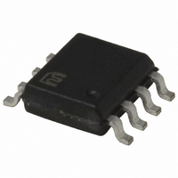
MIC4103YM Micrel Inc, MIC4103YM Datasheet - Page 11

MIC4103YM
Manufacturer Part Number
MIC4103YM
Description
IC MOSFET DRIVER 100V CMOS 8SOIC
Manufacturer
Micrel Inc
Specifications of MIC4103YM
Configuration
Half Bridge
Input Type
Non-Inverting
Delay Time
24ns
Current - Peak
2A
Number Of Configurations
1
Number Of Outputs
2
High Side Voltage - Max (bootstrap)
118V
Voltage - Supply
9 V ~ 16 V
Operating Temperature
-40°C ~ 125°C
Mounting Type
Surface Mount
Package / Case
8-SOIC (3.9mm Width)
Device Type
MOSFET
Module Configuration
Half Bridge
Peak Output Current
3A
Output Resistance
2.5ohm
Input Delay
24ns
Output Delay
24ns
Supply Voltage Range
9V To 16V
Driver Case
RoHS Compliant
Lead Free Status / RoHS Status
Lead free / RoHS Compliant
Other names
576-1589
High-Side Driver and Bootstrap Circuit
A block diagram of the high-side driver and bootstrap
circuit is shown in Figure 4. This driver is designed to drive
a floating N-channel MOSFET, whose source terminal is
referenced to the HS pin.
A low-power, high-speed, level shifting circuit isolates the
low-side (VSS pin) referenced circuitry from the high-side
(HS pin) referenced driver. Power to the high-side driver
and UVLO circuit is supplied by the bootstrap circuit while
the voltage level of the HS pin is shifted high.
The bootstrap circuit consists of an internal diode and
external capacitor, C
synchronous buck converter shown in Figure 5, the HS pin
is at ground potential while the low-side MOSFET is on.
The internal diode allows capacitor C
V
drop of the internal diode). After the low-side MOSFET is
turned off and the HO pin turns on, the voltage across
capacitor C
MOSFET. As the upper MOSFET turns on, voltage on the
HS pin rises with the source of the high-side MOSFET until
it reaches V
diode is reverse biased preventing capacitor C
discharging.
Micrel
November 2010
DD
Figure 4. High-Side Driver and Bootstrap Circuit Block
− V
D
during this time (where V
B
IN
is applied to the gate of the upper external
. As the HS and HB pin rise, the internal
B
. In a typical application, such as the
Diagram
D
is the forward voltage
B
to charge up to
B
from
11
Power Dissipation Considerations
Power dissipation in the driver can be separated into three
areas:
Bootstrap Circuit Power Dissipation
Power dissipation of the internal bootstrap diode primarily
comes from the average charging current of the C
capacitor times the forward voltage drop of the diode.
Secondary sources of diode power dissipation are the
reverse leakage current and reverse recovery effects of
the diode.
The average current drawn by repeated charging of the
high-side MOSFET is calculated by:
The average power dissipated by the forward voltage drop
of the diode equals:
C
I
where
Pdiode
where
VDD
F
HI
LI
Figure 5. High-Side Driver and Bootstrap Circuit
•
•
•
(
AVE
Internal diode dissipation in the bootstrap circuit
Internal driver dissipation
Quiescent current dissipation used to supply the
internal logic and control functions.
Level
)
shift
:
:
fwd
f
Q
V
=
S
Vdd
F
gate
Q
=
=
=
gate
gate
I
Diode
F
=
(
Vss
AVE
×
Total
drive
f
S
HB
)
forward
×
Gate
V
HO
switching
C
HS
LO
F
B
Charge
voltage
frequency
Vin
at
drop
V
M9999-110910-B
Q1
Q2
MIC4103/4104
HB
Lout
B


