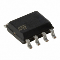
STSR2PCD-TR STMicroelectronics, STSR2PCD-TR Datasheet - Page 3

STSR2PCD-TR
Manufacturer Part Number
STSR2PCD-TR
Description
IC SYNC RECT SMART DRIVER 8 SOIC
Manufacturer
STMicroelectronics
Datasheet
1.STSR2PCD-TR.pdf
(12 pages)
Specifications of STSR2PCD-TR
Configuration
Low-Side
Input Type
Non-Inverting
Current - Peak
2A
Number Of Configurations
2
Number Of Outputs
2
Voltage - Supply
4.5 V ~ 5.5 V
Operating Temperature
-40°C ~ 125°C
Mounting Type
Surface Mount
Package / Case
8-SOIC (3.9mm Width)
Output Voltage
0.16 V
Operating Temperature Range
- 40 C to + 125 C
Mounting Style
SMD/SMT
Lead Free Status / RoHS Status
Lead free / RoHS Compliant
Delay Time
-
High Side Voltage - Max (bootstrap)
-
Lead Free Status / Rohs Status
Lead free / RoHS Compliant
Other names
497-2154-2
Available stocks
Company
Part Number
Manufacturer
Quantity
Price
Part Number:
STSR2PCD-TR
Manufacturer:
ST
Quantity:
20 000
PIN DESCRIPTION
Pin N°
1
2
3
4
5
6
7
8
OUT
OUT
PWRGND
SGLGND
SET
Symbol
INHIBIT
V
CK
GATE1
CC
GATE2
ANT2
Gate Drive signal for Rectifier MOSFET. Anticipation (t
OUT
The supply voltage range from 4.5V to 5.5V allows applications with logic gate
threshold mosfets. UVLO feature guarantees proper start-up while it avoids
undesirable driving during eventual dropping of the supply voltage.
The voltage on this pin sets the anticipation (t
is possible to choose among three different anticipation times by discrete
partitioning of the supply voltage.
This input provides synchronization for IC’s operations, being the transitions
between the two output conditions based on a positive threshold, equal for the
two slopes. A smart internal control logic mechanism using a 15MHz internal
oscillator generates proper anticipation timing at the turn-off of each output. This
feature allows safe turn-off of Synchronous Rectifiers avoiding any eventual
shoot-through situation on secondary side at both transitions. Smart clock
revelation mechanism makes these operations independent by false triggering
pulses generated in light load conditions and by particular demagnetization
techniques.Absolute maximum voltage rating of the pin can be exceeded limiting
the current flowing into the pin to 10mA max.
This input enables OUT
threshold voltage (V
minimum conduction time (t
is possible to turn off the freewheeling MOSFET when the current through it tends
to reverse, allowing discontinuous conduction mode and providing protection to
the converter from eventual sinking current from the load.Absolute maximum
voltage rating of the pin can be exceeded limiting the current flowing into the pin
to 10mA max.
Reference for all the control logic signals. This pin is completely separated from
the PWRGND to prevent eventual disturbances to affect the control logic.
Gate Drive signal for Freewheeling MOSFET. Anticipation [t
OUT
Reference for power signals, this pin carries the full peak currents for the two
outputs.
GATE1
GATE2
is provided when the clock input goes to low level.
is provided when the clock input goes to high level.
INHIBIT
GATE2
<V
ON(GATE2)
H
Name and Function
to work when its voltage is lower than the negative
). If V
INHIBIT
). In typical forward converter application, it
>V
ANT1
H
the OUT
) in turning off the OUT
ANT1
GATE2
STSR2P/STSR2PM
) in turning off
ANT2
will be high for a
] in turning off
GATE2
3/12
. It


