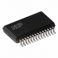
UBA2035TS/N1,118 NXP Semiconductors, UBA2035TS/N1,118 Datasheet - Page 5

UBA2035TS/N1,118
Manufacturer Part Number
UBA2035TS/N1,118
Description
IC DVR HF FULL BRIDGE 28-SSOP
Manufacturer
NXP Semiconductors
Type
HID Lamp Controllerr
Datasheet
1.UBA2035TSN1118.pdf
(13 pages)
Specifications of UBA2035TS/N1,118
Frequency
100kHz
Current - Supply
500µA
Current - Output
200mA
Voltage - Supply
10.5 V ~ 13.5 V
Operating Temperature
-40°C ~ 125°C
Package / Case
28-SSOP
Supply Voltage (min)
10.5 V
Supply Current
0.8 mA
Maximum Operating Temperature
+ 125 C
Mounting Style
SMD/SMT
Bridge Type
Full Bridge
Minimum Operating Temperature
- 40 C
Number Of Drivers
3
Number Of Outputs
3
Lead Free Status / RoHS Status
Lead free / RoHS Compliant
Lead Free Status / RoHS Status
Lead free / RoHS Compliant, Lead free / RoHS Compliant
Other names
935284377118
NXP Semiconductors
UBA2035_1
Product data sheet
7.4 Non-overlap time
7.5 Start-up delay
Table 3.
Gate driver output voltages as function of the logical levels at the pins BD, SU, DD and CLK.
[1]
[2]
If there is no external clock available, the internal oscillator can be used. The design
equation for the bridge oscillator frequency is shown in
R
VDD and C
V
The clock signal, either coming from pin RC or pin CLK, can be divided by two in order to
obtain a 50 % duty cycle gate drive signal. This can be achieved by applying a voltage to
the DD input lower than V
In the full bridge configuration the non-overlap time is defined as the time between turning
off the two conducting MOSFETs and turning on the two other MOSFETs. The (very
small) non-overlap time is internally fixed to t
a very small phase angle between the load current and the full bridge voltage (pins SHL
and SHR). This can be beneficial for HID systems in which the lamp is ignited via a
resonance network.
A simple resistor-capacitor (RC) filter (R between pin VDD and pin SU; C between pin SU
and pin SGND) or a control signal from a processor can be used to create a start-up
delay. This can be beneficial for those applications in which building up the high voltage
takes more time. A start-up delay will ensure that the HID system will not start up before
this high voltage has been reached.
Device
state
Start-up
state
Oscillation
state
f
bridge
SS(CLK)
osc
If pin DD = 0 the bridge enters the state (oscillation state and pin BD = 0 and pin SU = 1) in the predefined
position: V
Only if the level of pin CLK changes from logical 1 to 0, the level of outputs GHL, GHR, GLL and GLR
changes.
and C
=
can be connected to SGND.
-------------------------------------------- -
K
Driver
osc
osc
osc
GHL
BD
1
0
1
0
0
0
0
are external components connected to the RC pin (R
connected to pin SGND). In this situation the pins V
= V
R
1
osc
FSL
SU
-
-
-
0
1
1
1
, V
Rev. 01 — 31 October 2008
C
GLR
osc
IL(DD)
DD
-
-
-
-
1
1
0
= V
[1]
VDD
(e.g. connect pin DD to pin SGND).
CLK
-
-
-
-
1
0
1
, V
GLL
0
[2]
= V
PGND
GHL
0 (= V
0 (= V
0 (= V
0 (= V
0 (= V
1 (= V
GHL
no
and V
, which allows a HID system to operate with
HF Full bridge control IC for HID lighting
SHL
SHL
SHL
SHL
SHL
FSL
GHR
)
)
)
)
)
)
GHR
0 (= V
0 (= V
0 (= V
0 (= V
1 (= V
0 (= V
GHR
= V
Equation
SHR
SHR
SHR
SHR
SHR
FSR
SHR
.
)
)
)
)
)
)
1.
GLL
0 (= V
1 (= V
0 (= V
1 (= V
1 (= V
0 (= V
GLL
DD(CLK)
osc
UBA2035
connected to pin
PGND)
VDD
PGND
VDD
VDD
PGND
© NXP B.V. 2008. All rights reserved.
, CLK, and
)
)
)
) 0 (= V
) 1 (= V
GLR
0 (= V
1 (= V
1 (= V
0 (= V
GLR
PGND
VDD
PGND
VDD
PGND
VDD
5 of 13
)
)
)
(1)
)
)
)


