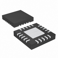
MAX6964ATG+T Maxim Integrated Products, MAX6964ATG+T Datasheet - Page 2

MAX6964ATG+T
Manufacturer Part Number
MAX6964ATG+T
Description
IC LED DRIVER LINEAR 24-TQFN
Manufacturer
Maxim Integrated Products
Type
Linear (I²C Interface)r
Datasheet
1.MAX6964AEG.pdf
(23 pages)
Specifications of MAX6964ATG+T
Topology
Open Drain, PWM
Number Of Outputs
17
Internal Driver
Yes
Type - Primary
Backlight, LED Blinker
Type - Secondary
RGB, White LED
Frequency
400kHz
Voltage - Supply
2 V ~ 3.6 V
Voltage - Output
7V
Mounting Type
Surface Mount
Package / Case
24-TQFN Exposed Pad
Operating Temperature
-40°C ~ 125°C
Current - Output / Channel
50mA
Internal Switch(s)
Yes
Number Of Segments
12
Low Level Output Current
50 mA
Operating Supply Voltage
2 V to 3.6 V
Maximum Supply Current
122.1 uA
Maximum Power Dissipation
1666 mW
Maximum Operating Temperature
+ 125 C
Mounting Style
SMD/SMT
Minimum Operating Temperature
- 40 C
Lead Free Status / RoHS Status
Lead free / RoHS Compliant
Efficiency
-
Lead Free Status / Rohs Status
Details
ABSOLUTE MAXIMUM RATINGS
Voltage (with respect to GND)
V+ .............................................................................-0.3V to +4V
SCL, SDA, AD0, BLINK, RST ...................................-0.3V to +6V
O0–O16 ....................................................................-0.3V to +8V
DC Current on O0 to O16 ...................................................55mA
DC Current on SDA.............................................................10mA
Maximum GND Current ....................................................350mA
ELECTRICAL CHARACTERISTICS
(Typical Operating Circuit, V+ = 2V to 3.6V, T
(Note 1)
17-Output LED Driver/GPO with
Intensity Control and Hot-Insertion Protection
Stresses beyond those listed under “Absolute Maximum Ratings” may cause permanent damage to the device. These are stress ratings only, and functional
operation of the device at these or any other conditions beyond those indicated in the operational sections of the specifications is not implied. Exposure to
absolute maximum rating conditions for extended periods may affect device reliability.
2
Operating Supply Voltage
Output Load External Supply
Voltage
Standby Current
(Interface Idle, PWM Disabled)
Supply Current
(Interface Idle, PWM Enabled)
Supply Current
(Interface Running, PWM
Disabled)
Supply Current
(Interface Running, PWM
Enabled)
Input High Voltage
SDA, SCL, AD0, BLINK, RST
Input Low Voltage
SDA, SCL, AD0, BLINK, RST
Input Leakage Current
SDA, SCL, AD0, BLINK, RST
Input Capacitance
SDA, SCL, AD0, BLINK, RST
_______________________________________________________________________________________
PARAMETER
SYMBOL
I
V
IH
V
V
V+
EXT
I
I
I
I
, I
+
+
+
+
IH
IL
IL
A
S C L and S D A at V + ; other
d i g i tal i np uts at V + or GN D ;
P WM i ntensi ty contr ol d i sab l ed
S C L and S D A at V + ; other
d i g i tal i np uts at V + or GN D ;
P WM i ntensi ty contr ol d i sab l ed
f
inputs at V+ or GND; PWM
intensity control enabled
f
inputs at V+ or GND; PWM
intensity control enabled
0 ≤ input voltage ≤ 5.5V
SCL
SCL
= T
MIN
= 400kHz; other digital
= 400kHz; other digital
to T
MAX
, unless otherwise noted. Typical values are at V+ = 3.3V, T
CONDITIONS
Continuous Power Dissipation (T
Operating Temperature Range .........................-40°C to +125°C
Junction Temperature ......................................................+150°C
Storage Temperature Range .............................-65°C to +150°C
Lead Temperature (soldering, 10s) .................................+300°C
24-Pin QSOP (derate 9.5mW/°C over +70°C)..............761mW
24-Pin QFN (derate 20.8mW/°C over +70°C) ............1666mW
T
T
T
T
T
T
T
T
T
T
T
T
A
A
A
A
A
A
A
A
A
A
A
A
= +25°C
= -40°C to +85°C
= T
= +25°C
= -40°C to +85°C
= T
= +25°C
= -40°C to +85°C
= T
= +25°C
= -40°C to +85°C
= T
MIN
MIN
MIN
MIN
to T
to T
to T
to T
MAX
MAX
MAX
MAX
0.7 x
MIN
-0.2
2.0
V+
A
0
= +70°C)
TYP
1.2
8.5
50
57
8
102.4
110.2
117.4
122.1
MAX
0.3 x
+0.2
15.1
16.5
17.2
95.3
99.2
3.6
2.3
2.6
3.3
V+
7
A
= +25°C.)
UNITS
µA
µA
µA
µA
µA
pF
V
V
V
V


