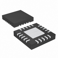
MAX6964ATG+T Maxim Integrated Products, MAX6964ATG+T Datasheet - Page 12

MAX6964ATG+T
Manufacturer Part Number
MAX6964ATG+T
Description
IC LED DRIVER LINEAR 24-TQFN
Manufacturer
Maxim Integrated Products
Type
Linear (I²C Interface)r
Datasheet
1.MAX6964AEG.pdf
(23 pages)
Specifications of MAX6964ATG+T
Topology
Open Drain, PWM
Number Of Outputs
17
Internal Driver
Yes
Type - Primary
Backlight, LED Blinker
Type - Secondary
RGB, White LED
Frequency
400kHz
Voltage - Supply
2 V ~ 3.6 V
Voltage - Output
7V
Mounting Type
Surface Mount
Package / Case
24-TQFN Exposed Pad
Operating Temperature
-40°C ~ 125°C
Current - Output / Channel
50mA
Internal Switch(s)
Yes
Number Of Segments
12
Low Level Output Current
50 mA
Operating Supply Voltage
2 V to 3.6 V
Maximum Supply Current
122.1 uA
Maximum Power Dissipation
1666 mW
Maximum Operating Temperature
+ 125 C
Mounting Style
SMD/SMT
Minimum Operating Temperature
- 40 C
Lead Free Status / RoHS Status
Lead free / RoHS Compliant
Efficiency
-
Lead Free Status / Rohs Status
Details
17-Output LED Driver/GPO with
Intensity Control and Hot-Insertion Protection
Table 4. Configuration Register (continued)
Table 5. Blink Controls
X = Don’t care.
12
X = Don’t care.
is set by registers 0x10–0x17 for ports O0
through O15 when configured as outputs,
Disable global intensity control—intensity
and by D3–D0 of register 0x0E for output
Enable global intensity control—intensity
for all ports configured as outputs is set
BLINK ENABLE
O16 output is high impedance (blink is
O16 output is high impedance during
O16 output is high impedance during
O 16 outp ut i s l ow d ur i ng b l i nk p hase 0
O 16 outp ut i s l ow d ur i ng b l i nk p hase 1
O16 output is low (blink is disabled)
Read back BLINK input pin status;
Read back BLINK input pin status;
______________________________________________________________________________________
Read back device configuration
FLAG
by D3–D0 of register 0x0E
Write device configuration
E
0
1
CONFIGURATION
blink phase 0
blink phase 1
input is high
REGISTER
input is low
disabled)
BLINK FLIP
FLAG
B
X
0
0
1
1
BLINK INPUT
R/W
—
—
—
—
—
—
—
—
0
1
1
1
PIN
X
0
1
0
1
ADDRESS
CODE
(hex)
0x0F
BLINK FLIP FLAG
BLINK INPUT PIN
D7
X
0
X
X
X
X
X
X
X
X
X
X
EXOR
X
0
1
1
0
BLINK
D6
X
X
X
X
X
X
X
X
0
1
O1
D5
X
X
X
X
X
X
0
1
X
X
FUNCTION
Disabled
Enabled
BLINK
REGISTER DATA
D4
O0
X
X
X
X
X
X
0
1
0
1
D3
X
X
X
X
X
0
0
0
0
0
0
0
OUTPUT REGISTERS
D2
Blink phase 0
Blink phase 0
Blink phase 1
Blink phase 1
Blink phase 0
G
0
1
X
X
X
X
X
X
X
X
USED
D1
B
X
X
X
X
X
X
X
X
X
X
D0
E
X
X
X
X
0
0
1
1
1
1


