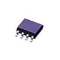
MXHV9910BE Clare, MXHV9910BE Datasheet - Page 4

MXHV9910BE
Manufacturer Part Number
MXHV9910BE
Description
IC LED DRIVER HIGH BRIGHT 8-SOIC
Manufacturer
Clare
Type
HBLED Driverr
Datasheet
1.MXHV9910BTR.pdf
(11 pages)
Specifications of MXHV9910BE
Topology
AC DC Offline Switcher, PWM, Step-Down (Buck)
Number Of Outputs
1
Internal Driver
No
Type - Primary
Backlight
Type - Secondary
High Brightness LED (HBLED), RGB
Frequency
51kHz ~ 77kHz
Voltage - Supply
8 V ~ 450 V
Voltage - Output
7.8V
Mounting Type
Surface Mount
Package / Case
8-SOIC (3.9mm Width) Exposed Pad, 8-eSOIC. 8-HSOIC
Operating Temperature
-40°C ~ 85°C
Internal Switch(s)
No
Efficiency
90%
Operating Supply Voltage
8 V to 450 V
Maximum Power Dissipation
2.5 W
Maximum Operating Temperature
+ 85 C
Mounting Style
SMD/SMT
Minimum Operating Temperature
- 40 C
Lead Free Status / RoHS Status
Lead free / RoHS Compliant
Current - Output / Channel
-
MXHV9910
1.4 Recommended Operating Conditions
1.5 Electrical Characteristics
Unless otherwise specified, all electrical specifications are provided for T
1.6 Thermal Characteristics
1
4
Input Voltage Range
PWMD Frequency
Operating Temperature
Input
Input DC Voltage Range
Shut-Down Mode Supply Current
Maximum Voltage to V
Regulator
Internal Voltage Regulator
V
for External Circuitry
V
PWM Dimming
PWMD Input Low Voltage
PWMD Input High Voltage
PWMD Pull-Down Resistance
Current Sense Comparator
Current Sense (CS) Input Current
Current Sense Threshold Voltage
Current Sense Blanking Interval
Delay from CS Trip to Gate Low
Oscillator
Oscillator Frequency (Gate Driver)
Gate Driver
Gate High Output Voltage
Gate Low Output Voltage
Gate Output Rise Time
Gate Output Fall Time
Thermal Resistance,
Junction-to-Ambient
CS Low
CS High
Use of a four-layer PCB can improve thermal dissipation (reference EIA/JEDEC JESD51-5).
DD
DD
Current Available
Load Regulation
Parameter
Parameter
Parameter
DD
Pin
External Voltage applied to V
PWMD to GND, V
SOIC-8 With Thermal Pad (BE)
SOIC-8 W/O Thermal Pad (B)
Symbol
f
V
PWMD
IN
GATE Output=Open
V
T
-40°C < T
V
V
IN
DC Input Voltage
A
=12V, V
V
V
IN
IN
C
C
I
IN
IN
OUT
I
Conditions
R
R
R
GATE
GATE
OUT
I
=15V to 450V,
=15V, I
DD(ext)
=8V to 450V
=8V to 450V
CS=V
T
T
T
CS=0V
Package
=400kΩ
=400kΩ
=400kΩ
= -10mA
=10mA
-
PWMD
=500pF
=500pF
A
L
DD
IN
=0,
< 85°C
=1mA
www.clare.com
Minimum
=15 to 450V
=V
-40
8
-
DD
DD
Pin
1
Nominal
V
V
V
500
V
V
Symbol
Symbol
V
I
t
EN
t
GATE
GATE
-
-
DD(ext)
CS(high)
EN
BLANK
ΔV
DELAY
R
I
t
t
DDmax
V
R
INSD
RISE
FALL
V
I
I
f
θJA
DD
(high)
IH
EN
IL
S
(low)
IN
DD
(hi)
(lo)
Maximum
A
=25°C.
450
+85
Minimum
Minimum
V
-
DD
200
7.2
2.4
70
51
8
-
-
-
-
-
-
-
-
-
-
-
-
-
-
-0.3
Unit
V
Hz
°C
Typical
Typical
DC
0.03
115
400
300
128
-45
0.3
7.8
64
16
50
0
7
-
-
-
-
-
-
-
-
Maximum
Maximum
450
200
150
±15
280
0.6
8.4
0.5
-90
0.3
12
77
2
-
-
-
-
-
-
-
-
°C/W
Unit
V
V
Unit
kHz
mA
mA
mV
mV
kΩ
μA
ns
ns
ns
DC
V
DC
V
V
R01


