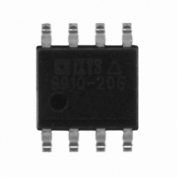
MXHV9910B Clare, MXHV9910B Datasheet - Page 6

MXHV9910B
Manufacturer Part Number
MXHV9910B
Description
IC LED DRIVER HIGH BRIGHT 8-SOIC
Manufacturer
Clare
Type
HBLED Driverr
Datasheet
1.MXHV9910BTR.pdf
(11 pages)
Specifications of MXHV9910B
Topology
AC DC Offline Switcher, PWM, Step-Down (Buck)
Number Of Outputs
1
Internal Driver
No
Type - Primary
Backlight
Type - Secondary
High Brightness LED (HBLED), RGB
Frequency
51kHz ~ 77kHz
Voltage - Supply
8 V ~ 450 V
Voltage - Output
7.8V
Mounting Type
Surface Mount
Package / Case
8-SOIC (3.9mm Width)
Operating Temperature
-40°C ~ 85°C
Internal Switch(s)
No
Efficiency
90%
Lead Free Status / RoHS Status
Lead free / RoHS Compliant
Current - Output / Channel
-
MXHV9910
Figure 3 MXHV9910 Waveforms (From Application Circuit in Figure 6)
The MXHV9910 has an internal voltage regulator that
can work with input voltages ranging from 12V
450 V
is greater than 12V
regulates this voltage down to a typical 7.8V. The V
pin is the internal regulator output pin and must be
bypassed by a low ESR capacitor, typically 0.1μF, to
provide a low impedance path for high frequency
switching noise.
The MXHV9910 driver does not require the bulky
start-up resistors typically needed for off-line
controllers. An internal voltage regulator provides
sufficient voltage and current to power the internal IC
circuits. This voltage is also available at the V
and can be used as bias voltage for external circuitry.
The internal voltage regulator can by bypassed by
applying an external DC voltage to the V
slightly higher than the internal regulator’s maximum
output voltage. This feature reduces power dissipation
of the integrated circuit and is more suitable in isolated
applications where an auxiliary transformer winding
could be used to supply V
The total input current drawn by the V
the integrated circuit quiescent current, which is
0.6mA maximum, plus the gate driver current. The
gate driver current is dependant on the switching
frequency and the gate charge of the external power
MOSFET.
6
2.2.1 Input Voltage Regulator
DC
. When the input voltage applied at the V
DC
, the internal voltage regulator
DD
.
IN
pin is equal to
DD
pin that is
DD
DC
pin,
IN
to
www.clare.com
pin
DD
The following equation can be used to approximate
the V
Where Q
power MOSFET, and f
frequency.
The peak LED current is set by an external current
sense resistor connected from the CS pin to ground.
The value of the current sense resistor is calculated
based on the desired average LED current, the current
sense threshold, and the inductor ripple current.
The inductor is typically selected to be large enough to
keep the ripple current (the peak-to-peak difference in
the inductor current waveform) to less than 30% of the
average LED current. Factoring in this ripple current
requirement, the current sense resistor can be
determined by:
Where:
•
•
•
The power dissipation rating of the sense resistor can
be found with the following formula:
V
r
I
LED
iout
csth
2.2.2 Current Sense Resistor
IN
= inductor ripple = 0.3
I
= average LED current
IN
= nominal current sense threshold = 0.25V
input current:
≈
GATE
0.6mA
R
sense
is the total gate charge of the external
+
=
(
P
Q
-------------------------------------------------------------
[
=
GATE
Time Scale: 5μs/div
CH1:
50mA/div
F
Max 77mA
CH2:
10V/div
CH3:
5mV/div x 10
1
S
S
+
I
LED
is the switching oscillator
65kHz
(
0.5
×
2
f
S
×
×
)
V
R
r
csth
iout
sense
)
] I
×
LED
R01


