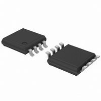
PCA9632DP1,118 NXP Semiconductors, PCA9632DP1,118 Datasheet - Page 6

PCA9632DP1,118
Manufacturer Part Number
PCA9632DP1,118
Description
IC LED DRIVER RGBA 8-TSSOP
Manufacturer
NXP Semiconductors
Type
RGBA LED Driverr
Datasheet
1.PCA9632TK118.pdf
(38 pages)
Specifications of PCA9632DP1,118
Package / Case
8-TSSOP
Topology
Open Drain, PWM
Number Of Outputs
4
Internal Driver
Yes
Type - Primary
Backlight, LED Blinker
Type - Secondary
RGBA
Frequency
1MHz
Voltage - Supply
2.3 V ~ 5.5 V
Voltage - Output
5.5V
Mounting Type
Surface Mount
Operating Temperature
-40°C ~ 85°C
Current - Output / Channel
25mA
Internal Switch(s)
Yes
Number Of Segments
4
Low Level Output Current
100000 uA
Operating Supply Voltage
2.3 V to 5.5 V
Maximum Supply Current
150 uA
Maximum Power Dissipation
400 mW
Maximum Operating Temperature
+ 85 C
Mounting Style
SMD/SMT
Minimum Operating Temperature
- 40 C
Lead Free Status / RoHS Status
Lead free / RoHS Compliant
Efficiency
-
Lead Free Status / Rohs Status
Lead free / RoHS Compliant
Other names
935284899118
PCA9632DP1-T
PCA9632DP1-T
PCA9632DP1-T
PCA9632DP1-T
Available stocks
Company
Part Number
Manufacturer
Quantity
Price
Part Number:
PCA9632DP1,118
Manufacturer:
NXP/恩智浦
Quantity:
20 000
NXP Semiconductors
7. Functional description
PCA9632_3
Product data sheet
7.1.1 Regular I
7.1 Device addresses
Table 3.
[1]
Refer to
Following a START condition, the bus master must output the address of the slave it is
accessing.
There are a maximum of 4 possible programmable addresses using the 2 hardware
address pins for the 10-pin version and just one fixed address for the 8-pin version.
The I
internal pull-up resistors are incorporated on the hardware selectable address pins and
they must be pulled HIGH or LOW (10-pin versions only).
Remark: Using reserved I
devices are on the bus and/or the bus will be open to other I
date. In a closed system where the designer controls the address assignment these
addresses can be used since the PCA9632 treats them like any other address. The
LED All Call, Software Reset and PCA9564 or PCA9665 slave address (if on the bus) can
never be used for individual device addresses.
Symbol
LED0
LED1
LED2
LED3
A0
V
A1
SCL
SDA
V
•
•
•
•
SS
DD
HVSON10 package die supply ground is connected to both the V
V
and board-level performance, the exposed pad needs to be soldered to the board using a corresponding
thermal pad on the board, and for proper heat conduction through the board thermal vias need to be
incorporated in the PCB in the thermal pad region.
PCA9632 LED All Call address (1110 000) or Software Reset (0000 0110) which are
active on start-up
PCA9564 (0000 000) or PCA9665 (1110 000) slave address which is active on
start-up
‘reserved for future use’ I
slave devices that use the 10-bit addressing scheme (1111 0XX)
2
SS
C-bus slave address of the PCA9632 is shown in
pin must be connected to supply ground for proper device operation. For enhanced thermal, electrical,
Figure 1 “Block diagram of
2
Pin description for TSSOP10 and HVSON10
C-bus slave address
Pin
1
2
3
4
5
6
7
8
9
10
[1]
Type
O
O
O
O
I
power supply
I
I
I/O
power supply
Rev. 03 — 15 July 2008
2
C-bus addresses will interfere with other devices, but only if the
2
C-bus addresses (0000 011, 1111 1XX)
Description
LED driver 0
LED driver 1
LED driver 2
LED driver 3
address input 0
supply ground
address input 1
serial clock line
serial data line
supply voltage
PCA9632”.
4-bit Fm+ I
Figure
SS
2
pin and the exposed center pad. The
C-bus low power LED driver
2
C-bus systems at some later
6. To conserve power, no
PCA9632
© NXP B.V. 2008. All rights reserved.
6 of 38


