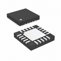
LTC3209EUF-1#PBF Linear Technology, LTC3209EUF-1#PBF Datasheet - Page 7

LTC3209EUF-1#PBF
Manufacturer Part Number
LTC3209EUF-1#PBF
Description
IC LED DRIVR QVGA DISPLAY 20-QFN
Manufacturer
Linear Technology
Type
QVGA Display (I²C Interface)r
Datasheet
1.LTC3209EUF-1PBF.pdf
(20 pages)
Specifications of LTC3209EUF-1#PBF
Topology
Step-Up (Boost), Switched Capacitor (Charge Pump)
Number Of Outputs
8
Internal Driver
Yes
Type - Primary
Backlight
Type - Secondary
White LED
Frequency
850kHz
Voltage - Supply
2.9 V ~ 4.5 V
Mounting Type
Surface Mount
Package / Case
20-QFN
Operating Temperature
-40°C ~ 85°C
Internal Switch(s)
Yes
Efficiency
94%
Lead Free Status / RoHS Status
Lead free / RoHS Compliant
Voltage - Output
-
Current - Output / Channel
-
Available stocks
Company
Part Number
Manufacturer
Quantity
Price
PI FU CTIO S
CPO (Pin 1/Pin 1): Output of the Charge Pump Used to
Power LEDs. A 2.2µF X5R or X7R ceramic capacitor
should be connected to ground.
MAIN1-6 (Pins 2, 3, 4, 5, 6, 7, LTC3209-1): Current
Source Outputs for the MAIN Display White LEDs. The
LEDs on the MAIN display can be set from 0mA to 28mA
in 256 steps via software control and internal 8-bit linear
DAC. Each output can be disabled externally by connecting
the output to CPO. Setting data in REGA to 0 disables all
MAIN outputs.
MAIN1-5 (Pins 2, 3, 4, 5, 6, LTC3209-2): Current Source
Outputs for the MAIN Display White LEDs. The LEDs on the
MAIN display can be set from 0mA to 28mA in 256 steps
via software control and internal 8-bit linear DAC. Each
output can be disabled externally by connecting the output
to CPO. Setting data in REGA to 0 disables all MAIN
outputs.
AUX (Pin 8/Pin 7): Current Source Output for the AUX
Display LED. The LED current source can be set from 0mA
to 13.75mA in 4 steps via software control and internal 2-
bit DAC. AUX does not have dropout sensing and cannot
be disabled by connecting to CPO. This pin can also be
used as an I
V
Device. Two separate pins are used to isolate the charge
pump from the analog sections to reduce noise. Both pins
must be connected together externally and bypassed with
a single 2.2µF low ESR ceramic capacitor close to V
V
R
of LED current for all displays. The R
An external 24.3k resistor to ground sets the reference
currents for all display DACs and support circuits for nomi-
nal MAIN full-scale current of 28mA and total CAM full-scale
current of 400mA. The value for R
of 20k to 30k.
DV
Lines. This pin sets the logic reference level of the
LTC3209-1/LTC3209-2. Decouple DV
0.1µF capacitor. A UVLO circuit on the DV
registers to all 0s whenever DV
threshold.
BAT2,1
BAT2
REF
CC
U
(Pin 10/Pin 9): This pin controls the maximum amount
(Pin 11/Pin 10): Supply Voltage for All Digital I/O
may require a 0.1µF capacitor.
(Pins 9, 18/Pins 8, 18): Supply Voltage for the Entire
U
2
C controlled general purpose output.
U
(LTC3209-1/LTC3209-2)
CC
REF
REF
is below the UVLO
is limited to a range
CC
voltage is 1.23V.
CC
to GND with a
pin forces all
BAT1
.
CAM1-2 (Pins 11, 12, LTC3209-2): Current Source
Outputs for the CAM1 and CAM2 Display White LEDs. The
LEDs on the two CAM displays can each be set from 0mA
to 200mA in 16 steps via software control and internal
4-bit linear DAC. Two 4-bit registers are available. One is
used to program the high camera current and the second
the low camera current. These registers can be selected
via the serial port or the CAMHL pin. Each output can be
disabled by connecting the output to CPO. Setting data in
REGB to 0 disables both CAM outputs. (See Applications
Information).
CAM (Pin 12, LTC3209-1): Current Source Output for the
CAM Display White LED. The LED on the CAM display can
be set from 0mA to 400mA in 16 steps via software control
and internal 4-bit linear DAC. Two 4-bit registers are
available. One is used to program the high camera current
and the second the low camera current. These registers
can be selected via the serial port or the CAMHL pin. Each
output can be disabled by connecting the output to CPO.
Setting data in REGB to 0 disables the CAM output. (See
Applications Information).
CAMHL (Pin 13/Pin 13): This pin selects CAM high current
register when asserted high and CAM low current register
when low. The high to low transition automatically resets
the charge pump mode to 1x.
SDA (Pin 14/Pin 14): I
Serial data is shifted in one bit per clock to control the
LTC3209-1/LTC3209-2. The logic level is referenced to
DV
SCL (Pin 15/Pin 15): I
SCL is referenced to DV
C1P, C2P, C1M, C2M (Pins 20, 19, 17, 16/Pins 20, 19,
17, 16): Charge Pump Flying Capacitor Pins. A 2.2µF X7R
or X5R ceramic capacitor should be connected from C1P
to C1M and C2P to C2M.
Exposed Pad (Pin 21/Pin 21): System Ground. Connect
Exposed Pad to PCB ground plane.
CC
.
LTC3209-1/LTC3209-2
2
2
C Clock Input. The logic level for
CC
C Data Input for the Serial Port.
.
320912fa
7


