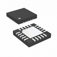
LTC3209EUF-1#PBF Linear Technology, LTC3209EUF-1#PBF Datasheet - Page 4

LTC3209EUF-1#PBF
Manufacturer Part Number
LTC3209EUF-1#PBF
Description
IC LED DRIVR QVGA DISPLAY 20-QFN
Manufacturer
Linear Technology
Type
QVGA Display (I²C Interface)r
Datasheet
1.LTC3209EUF-1PBF.pdf
(20 pages)
Specifications of LTC3209EUF-1#PBF
Topology
Step-Up (Boost), Switched Capacitor (Charge Pump)
Number Of Outputs
8
Internal Driver
Yes
Type - Primary
Backlight
Type - Secondary
White LED
Frequency
850kHz
Voltage - Supply
2.9 V ~ 4.5 V
Mounting Type
Surface Mount
Package / Case
20-QFN
Operating Temperature
-40°C ~ 85°C
Internal Switch(s)
Yes
Efficiency
94%
Lead Free Status / RoHS Status
Lead free / RoHS Compliant
Voltage - Output
-
Current - Output / Channel
-
Available stocks
Company
Part Number
Manufacturer
Quantity
Price
4
LTC3209-1/LTC3209-2
ELECTRICAL CHARACTERISTICS
temperature range, otherwise specifications are at T
unless otherwise noted.
PARAMETER
t
R
VR
RR
Note 1: Stresses beyond those listed under Absolute Maximum Ratings
may cause permanent damage to the device. Exposure to any Absolute
Maximum Rating condition for extended periods may affect device
reliability and lifetime.
Note 2: The LTC3209-1/LTC3209-2 are guaranteed to meet performance
specifications from 0°C to 70°C. Specifications over the –40°C to 85°C
ambient operating temperature range are assured by design,
characterization and correlation with statistical process controls.
TYPICAL PERFOR A CE CHARACTERISTICS
1V/DIV
SP
REF
V
0.65
0.60
0.55
0.50
0.45
0.40
0.35
REF
REF
CPO
–40
1x Mode Switch Resistance
vs Temperature
Mode Switch Fast Dropout Times
I
CPO
V
REGC C2 = Hi
BAT
= 200mA
–15
= 3.6V
1x
TEMPERATURE (°C)
V
V
BAT
BAT
10
= 3.3V
1ms/DIV
= 3.6V
1.5x
35
V
BAT
= 3.9V
W
60
2x
320912 G01
3209 G05
U
85
AC COUPLED
20mV/DIV
V
3.2
3.0
2.8
2.6
2.4
2.2
2.0
CPO
CONDITIONS
Spike Suppression Time
R
Reference Resistor Range
REF
–40
1.5x Mode Charge Pump Open-
Loop Output Resistance vs
Temperature (1.5V
A
V
V
C2 = C3 = C4 = 2.2µF
1.5x Mode CPO Ripple
= 24.3k
= 25
BAT
CPO
V
I
C
CPO
BAT
CPO
= 3V
= 4.2V
–15
= 200mA
= 3.6V
°
= 2.2µF
The
C. V
TEMPERATURE (°C)
●
BAT1,2
10
denotes the specifications which apply over the full operating
500ns/DIV
Note 3: 1.5x mode output impedance is defined as (1.5V
2x mode output impedance is defined as (2V
Note 4: Based on long term current density limitations. Assumes an
operating duty cycle of ≤ 10% under absolute maximum conditions for
duration less than 10 seconds. Max Charge Pump current for continuous
operation is 300mA.
Note 5: Based on long term current density limitations.
Note 6: All values are referrenced to V
Note 7: Guaranteed by design.
= 3.6V, DV
BAT
35
–V
CPO
60
)/I
CC
T
CPO
320912 G02
3209 G06
A
= 3V, R
= 25°C unless otherwise noted
85
AC COUPLED
REF
20mV/DIV
= 24.3k, C1 = C2 = C3 = C4 = 2.2
●
V
4.8
4.6
4.4
4.2
4.0
3.8
3.6
CPO
0
1.5x Mode CPO Voltage
vs Load Current
C2 = C3 = C4 = 2.2µF
V
2x Mode CPO Ripple
BAT
V
I
C
CPO
MIN
1.20
BAT
CPO
IH
50
20
= 3V
100
and V
= 200mA
3.1V
= 3.6V
= 2.2µF
3.2V
LOAD CURRENT (mA)
BAT
3.3V
IL
3.4V
1.23
TYP
3.5V
200
levels.
– V
500ns/DIV
CPO
)/I
300
BAT
OUT
MAX
1.26
30
– V
.
400
CPO
µ
3.6V
)/I
F,
320912fa
UNITS
3209 G07
320912 G03
OUT
500
kΩ
ns
.
V


