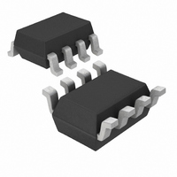
LT3590ESC8#TRPBF Linear Technology, LT3590ESC8#TRPBF Datasheet - Page 7

LT3590ESC8#TRPBF
Manufacturer Part Number
LT3590ESC8#TRPBF
Description
IC LED DRVR WHITE BCKLGT SC-70-8
Manufacturer
Linear Technology
Type
Backlight, White LEDr
Datasheet
1.LT3590ESC8TRMPBF.pdf
(16 pages)
Specifications of LT3590ESC8#TRPBF
Topology
PWM, Step-Down (Buck)
Number Of Outputs
1
Internal Driver
Yes
Type - Primary
Backlight
Type - Secondary
White LED
Frequency
650kHz ~ 1.05MHz
Voltage - Supply
4.5 V ~ 55 V
Voltage - Output
55V
Mounting Type
Surface Mount
Package / Case
SC-70-8
Operating Temperature
-40°C ~ 85°C
Current - Output / Channel
50mA
Internal Switch(s)
Yes
Efficiency
91%
Lead Free Status / RoHS Status
Lead free / RoHS Compliant
Available stocks
Company
Part Number
Manufacturer
Quantity
Price
OPERATION
The LT3590 uses a constant-frequency, current mode
control scheme to provide excellent line and load regula-
tion. Operation can be best understood by referring to the
Block Diagram.
At power-up, the bandgap reference, the start-up bias, and
the regulator are turned on. If CTRL is pulled higher than
150mV, the switching converter sub-blocks including the
oscillator, the PWM comparator and the error amplifi er
are also turned on. At the start of each oscillator cycle,
the power switch Q1 is turned on. Current fl ows through
the inductor and the switch to ground, ramping up as the
switch stays on. A voltage proportional to the switch cur-
rent is added to a stabilizing ramp and the resulting sum
is fed into the positive terminal of the PWM comparator.
When this voltage exceeds the level at the negative input of
the PWM comparator, the PWM logic turns off the power
switch. The level at the negative input of the PWM com-
parator is set by the error amplifi er EAMP , and is simply
an amplifi ed version of the difference between the V
V
the error amplifi er sets the correct peak current level in
inductor L1 to keep the output in regulation. The CTRL
pin is used to adjust the reference voltage.
The LT3590 enters into shutdown when CTRL is pulled
lower than 100mV.
Input Voltage Range
The minimum input voltage required to generate a particular
output voltage in an LT3590 application is limited by either
its 4.5V limit or by its maximum duty cycle. The duty cycle
is the fraction of time that the internal switch is on and is
determined by the input and output voltages:
Where V
(~0.8V) and V
at maximum load (~0.5V). Given DC
to minimum input voltage of:
LED
DC
V
IN MIN
voltage and the bandgap reference. In this manner,
(
=
V
D
IN
)
is the forward voltage drop of the catch diode
V
=
–
LED
(
SW
V
V
SW
LED
DC
+
is the voltage drop of the internal switch
V
MAX
+
D
+
V
V
D
D
)
+
V
SW
−
V
D
MAX
= 0.9, this leads
IN
and
The maximum input voltage is limited by the absolute
maximum V
Pulse-Skipping
For LED strings with a low number of LEDs (1, 2, or 3),
the LT3590 can drive currents without pulse-skipping as
long as the voltage across the LED and sense resistor is
greater than roughly 15% of the input supply voltage. If
the LED voltage plus sense resistor is less than 15% of
the input supply, the device will begin skipping pulses.
This will result in some low frequency ripple, although
the LED current remains regulated on an average basis
down to zero.
Discontinuous Current Mode
The CTRL pin, in conjunction with the sense resistor,
can be used to program the LED current as discussed
under Applications Information. The LT3590 can drive a
10-LED string at 10mA LED current operating in continu-
ous conduction mode, using the recommended external
components shown in the front page application circuit
with the sense resistor equal to 10Ω. As current is further
reduced, the regulator enters discontinuous conduction
mode. The photo in Figure 2 details circuit operation driving
ten LEDs at 2mA load. During the discharge phase, the
inductor current reaches zero. After the inductor current
reaches zero, the SW pin exhibits ringing due to the LC
tank circuit formed by the inductor in combination with
the switch and the diode capacitance. This ringing is not
harmful; far less spectral energy is contained in the ringing
than in the switch transitions. The ringing can be damped
by application of a 3kΩ resistor across the inductor, al-
though this will degrade effi ciency.
10mA/DIV
20V/DIV
V
IN
SW
I
L
Figure 2. Switching Waveforms
rating of 55V.
V
I
10 WHITE LEDs
L = 470μH (MURATA)
LED
IN
= 48V
= 2mA
400ns/DIV
3590 F02
LT3590
7
3590f


