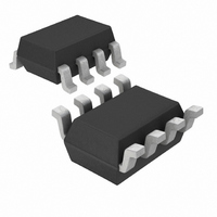
LT3590ESC8#TRPBF Linear Technology, LT3590ESC8#TRPBF Datasheet - Page 6

LT3590ESC8#TRPBF
Manufacturer Part Number
LT3590ESC8#TRPBF
Description
IC LED DRVR WHITE BCKLGT SC-70-8
Manufacturer
Linear Technology
Type
Backlight, White LEDr
Datasheet
1.LT3590ESC8TRMPBF.pdf
(16 pages)
Specifications of LT3590ESC8#TRPBF
Topology
PWM, Step-Down (Buck)
Number Of Outputs
1
Internal Driver
Yes
Type - Primary
Backlight
Type - Secondary
White LED
Frequency
650kHz ~ 1.05MHz
Voltage - Supply
4.5 V ~ 55 V
Voltage - Output
55V
Mounting Type
Surface Mount
Package / Case
SC-70-8
Operating Temperature
-40°C ~ 85°C
Current - Output / Channel
50mA
Internal Switch(s)
Yes
Efficiency
91%
Lead Free Status / RoHS Status
Lead free / RoHS Compliant
Available stocks
Company
Part Number
Manufacturer
Quantity
Price
PIN FUNCTIONS
BLOCK DIAGRAM
LT3590
SW (Pin 1/Pin 3): Switch Pin. Minimize trace area at this
pin to minimize EMI. Connect the inductor at this pin.
GND (Pins 2, 3, 4/Pin 2): Ground Pins. All ground pins
should be tied directly to local ground plane. Proper
soldering of these pins to the PCB ground is required to
achieve the rated thermal performance.
CTRL (Pin 5/Pin 1): Dimming and Shutdown Pin.
Connect it below 100mV to disable the switcher. As the
pin voltage is ramped from 0V to 1.5V, the feedback volt-
age (V
the LBD current.
6
I
LED
IN
CONTROL
0.1μF
=
- V
V
48V
1μF
C1
C3
IN
V
LED
IN
−
R
) ramps from 0mV to 200mV, controlling
1
V
VREG
LED
START-UP
CONTROL
REG
(SC70/DFN)
1.25V
VREF
CTRL
–
+
OSCILLATOR
GENERATOR
850kHz
RAMP
∑
–
+
PWM
Figure 1. Block Diagram
R
EAMP
S
VREG (Pin 6/Pin 6): Internally Generated 3.3V Regulated
Output Pin. Must be locally bypassed with a 0.1μF X5R
capacitor.
LED (Pin 7/Pin 5): Connection point for the anode of the
highest LED and the sense resistor.
V
passed.
Exposed Pad (NA/Pin 7): Ground. The Exposed Pad
should be soldered to the PCB ground to achieve the
rated thermal performance.
–
+
+
IN
Q
(Pin 8/Pin 4): Input Supply Pin. Must be locally by-
ISNS
+
–
GND
V
IN
A = 6.25
+
–
3590 F01
LED
SW
470μH
L1
R1
6.8Ω
V
OUT
C2
1μF
3590f


