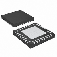
MAX16816ATJ+ Maxim Integrated Products, MAX16816ATJ+ Datasheet - Page 22

MAX16816ATJ+
Manufacturer Part Number
MAX16816ATJ+
Description
IC LED DRIVR HIGH BRIGHT 32-TQFN
Manufacturer
Maxim Integrated Products
Type
HBLED Driverr
Datasheet
1.MAX16816ATJ.pdf
(33 pages)
Specifications of MAX16816ATJ+
Topology
PWM, SEPIC, Step-Down (Buck), Step-Up (Boost)
Number Of Outputs
1
Internal Driver
Yes
Type - Primary
Automotive
Type - Secondary
High Brightness LED (HBLED)
Frequency
125kHz ~ 500kHz
Voltage - Supply
5.5 V ~ 76 V
Mounting Type
Surface Mount
Package / Case
32-TQFN Exposed Pad
Operating Temperature
-40°C ~ 125°C
Internal Switch(s)
Yes
Efficiency
90%
Low Level Output Current
76 mA
High Level Output Current
67 mA
Operating Supply Voltage
5.5 V to 76 V
Maximum Supply Current
4.5 mA
Maximum Power Dissipation
2758 mW
Maximum Operating Temperature
+ 125 C
Mounting Style
SMD/SMT
Minimum Operating Temperature
- 40 C
Lead Free Status / RoHS Status
Lead free / RoHS Compliant
Voltage - Output
-
Current - Output / Channel
-
Lead Free Status / Rohs Status
Details
The MAX16816 features built-in overvoltage protection,
overcurrent protection, HICCUP mode current-limit pro-
tection, and thermal shutdown. Overvoltage protection
is achieved by connecting OV to HI through a resistive
voltage-divider. HICCUP mode limits the power dissi-
pation in the external MOSFETs during severe fault
conditions. Internal thermal shutdown protection safely
turns off the converter when the IC junction temperature
exceeds +165°C.
The overvoltage protection (OVP) comparator com-
pares the voltage at OV with a 1.235V (typ) internal ref-
erence. When the voltage at OV exceeds the internal
reference, the OVP comparator terminates PWM
switching and no further energy is transferred to the
load. The MAX16816 reinitiates soft-start once the over-
voltage condition is removed. Connect OV to HI
through a resistive voltage-divider to set the overvolt-
age threshold at the output.
Connect OV to HI or to the high-side of the LEDs
through a resistive voltage-divider to set the overvolt-
age threshold at the output (Figure 4). The overvoltage
protection (OVP) comparator compares the voltage at
OV with a 1.235V (typ) internal reference. Use the fol-
lowing equation to calculate resistor values:
where V
and R
vent discharge of filter capacitors. This will prevent
unnecessary undervoltage and overvoltage conditions
during dimming.
The MAX16816 features load-dump protection up to 76V.
LED drivers using the MAX16816 can sustain single fault
load dump events. Repeated load dump events within
very short time intervals can cause damage to the dim-
ming MOSFET due to excess power dissipation.
The MAX16816 contains an internal temperature sensor
that turns off all outputs when the die temperature
exceeds +165°C. Outputs are enabled again when the
die temperature drops below +145°C.
Programmable Switch-Mode LED Driver
with Analog-Controlled PWM Dimming
22
______________________________________________________________________________________
OV2
OV
R
OV1
to be reasonably high value resistors to pre-
is the 1.235V OV threshold. Choose R
=
R
Setting the Overvoltage Threshold
OV2
x
⎛
⎜
⎝
V
OV_LIM
Overvoltage Protection
Load-Dump Protection
V
OV
Fault Protection
Thermal Shutdown
−
V
OV
⎞
⎟
⎠
OV1
The minimum required inductance is a function of oper-
ating frequency, input-to-output voltage differential, and
the peak-to-peak inductor current (ΔI
allows for a lower inductor value while a lower ΔI
requires a higher inductor value. A lower inductor value
minimizes size and cost, improves large-signal tran-
sient response, but reduces efficiency due to higher
peak currents and higher peak-to-peak output ripple
voltage for the same output capacitor. On the other
hand, higher inductance increases efficiency by reduc-
ing the ripple current, ΔI
due to extra turns can exceed the benefit gained from
lower ripple current levels, especially when the induc-
tance is increased without also allowing for larger
inductor dimensions. A good compromise is to choose
ΔI
saturating current is also important to avoid runaway
current during the output overload and continuous
short circuit. Select the I
mum peak current limit.
Buck configuration: In a buck configuration the average
inductor current does not vary with the input. The worst-
case peak current occurs at high input voltage. In this
case the inductance, L, for continuous conduction
mode is given by:
where V
switching frequency, and V
Figure 4. Setting the Overvoltage Threshold
L
equal to 30% of the full load current. The inductor
INMAX
V
LED+
R
R
L
OV1
OV2
=
is the maximum input voltage, f
Applications Information
V
OUT
V
INMAX
x V
SAT
(
L
INMAX
OUT
. However, resistive losses
OV
x f
to be higher than the maxi-
MAX16816
SW
Inductor Selection
is the output voltage.
AGND
−
x I
V
Δ
OUT
L
L
). Higher ΔI
)
SW
is the
L
L


