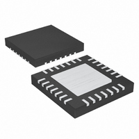
MAX16818ATI+ Maxim Integrated Products, MAX16818ATI+ Datasheet - Page 7

MAX16818ATI+
Manufacturer Part Number
MAX16818ATI+
Description
IC LED DRIVR PWM CONTROL 28-TQFN
Manufacturer
Maxim Integrated Products
Type
PWM Controlr
Datasheet
1.MAX16818ETI.pdf
(25 pages)
Specifications of MAX16818ATI+
Topology
High Side, Low Side, PWM, SEPIC, Step-Down (Buck), Step-Up (Boost)
Number Of Outputs
1
Internal Driver
No
Type - Primary
Automotive, Backlight
Type - Secondary
High Brightness LED (HBLED)
Frequency
125kHz ~ 1.5MHz
Voltage - Supply
4.75 V ~ 5.5 V, 7 V ~ 28 V
Voltage - Output
5.1V
Mounting Type
Surface Mount
Package / Case
28-TQFN Exposed Pad
Operating Temperature
-40°C ~ 125°C
Current - Output / Channel
30A
Internal Switch(s)
Yes
Low Level Output Current
4 A
High Level Output Current
4000000 uA (Typ)
Operating Supply Voltage
7 V to 28 V
Maximum Supply Current
5.5 mA
Maximum Power Dissipation
2758 mW
Maximum Operating Temperature
+ 125 C
Mounting Style
SMD/SMT
Minimum Operating Temperature
- 40 C
Lead Free Status / RoHS Status
Lead free / RoHS Compliant
Efficiency
-
Lead Free Status / Rohs Status
Lead free / RoHS Compliant
8, 22, 25
PIN
2, 7
10
11
12
13
14
15
16
17
18
19
20
1
3
4
5
6
9
RT/SYNC
CLKOUT
PGOOD
V_IOUT
EAOUT
NAME
PGND
SGND
N.C.
EAN
DIFF
CSN
CLP
BST
LIM
OVI
DH
EN
_______________________________________________________________________________________
DL
LX
1.5MHz, 30A High-Efficiency, LED Driver
Power-Supply Ground
No Connection. Not internally connected.
Low-Side Gate Driver Output
Boost Flying Capacitor Connection. Reservoir capacitor connection for the high-side MOSFET driver
supply. Connect a ceramic capacitor between BST and LX.
Source connection for the high-side MOSFET.
High-Side Gate Driver Output. Drives the gate of the high-side MOSFET.
Signal Ground. Ground connection for the internal control circuitry. Connect SGND and PGND
together at one point near the IC.
Oscillator Output. Rising edge of CLKOUT is phase-shifted from the rising edge of DH by 180°.
Power-Good Output
Output Enable. Drive high or leave unconnected for normal operation. Drive low to shut down the
power drivers. EN has an internal 15µA pullup current. Connect a capacitor from EN to SGND to
program the hiccup-mode duty cycle.
Switching Frequency Programming and Chip-Enable Input. Connect a resistor from RT/SYNC to
SGND to set the internal oscillator frequency. Drive RT/SYNC to synchronize the switching frequency
with external clock.
Voltage Source Output Proportional to the Inductor Current. The voltage at V_IOUT = 135 x I
Current-Limit Setting Input. Connect a resistor from LIM to SGND to set the hiccup current-limit
threshold. Connect a capacitor from LIM to SGND to ignore short output overcurrent pulses.
Overvoltage Protection. Connect OVI to DIFF. When OVI exceeds 12.7% above the programmed
output voltage, DH is latched low and DL is latched high. Toggle EN or recycle the input power to
reset the latch.
Current-Error Amplifier Output. Compensate the current loop by connecting an RC network to ground.
Voltage-Error Amplifier Output. Connect to the external compensation network.
Voltage-Error Amplifier Inverting Input
Differential Remote-Sense Amplifier Output. DIFF is the output of a precision unity-gain amplifier
whose inputs are SENSE+ and SENSE-.
Current-Sense Differential Amplifier Negative Input. The differential voltage between CSN and CSP is
amplified internally by the current-sense amplifier (gain = 34.5) to measure the inductor current.
with Rapid LED Current Pulsing
FUNCTION
Pin Description
LED
x R
S
.
7


