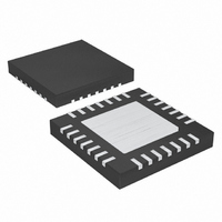
MAX16818ATI+ Maxim Integrated Products, MAX16818ATI+ Datasheet - Page 23

MAX16818ATI+
Manufacturer Part Number
MAX16818ATI+
Description
IC LED DRIVR PWM CONTROL 28-TQFN
Manufacturer
Maxim Integrated Products
Type
PWM Controlr
Datasheet
1.MAX16818ETI.pdf
(25 pages)
Specifications of MAX16818ATI+
Topology
High Side, Low Side, PWM, SEPIC, Step-Down (Buck), Step-Up (Boost)
Number Of Outputs
1
Internal Driver
No
Type - Primary
Automotive, Backlight
Type - Secondary
High Brightness LED (HBLED)
Frequency
125kHz ~ 1.5MHz
Voltage - Supply
4.75 V ~ 5.5 V, 7 V ~ 28 V
Voltage - Output
5.1V
Mounting Type
Surface Mount
Package / Case
28-TQFN Exposed Pad
Operating Temperature
-40°C ~ 125°C
Current - Output / Channel
30A
Internal Switch(s)
Yes
Low Level Output Current
4 A
High Level Output Current
4000000 uA (Typ)
Operating Supply Voltage
7 V to 28 V
Maximum Supply Current
5.5 mA
Maximum Power Dissipation
2758 mW
Maximum Operating Temperature
+ 125 C
Mounting Style
SMD/SMT
Minimum Operating Temperature
- 40 C
Lead Free Status / RoHS Status
Lead free / RoHS Compliant
Efficiency
-
Lead Free Status / Rohs Status
Lead free / RoHS Compliant
The main control loop consists of an inner current loop
(inductor current) and an outer LED current loop. The
MAX16818 uses an average current-mode control
scheme to regulate the LED current (Figure 7). The VEA
output provides the controlling voltage for the current
source. The inner current loop absorbs the inductor pole
reducing the order of the LED current loop to that of a
single-pole system. The major consideration when
designing the current control loop is making certain that
the inductor downslope (which becomes an upslope at
the output of the CEA) does not exceed the internal
ramp slope. This is a necessary condition to avoid sub-
harmonic oscillations similar to those in peak current
mode with insufficient slope compensation. This requires
that the resistance, R
ited, based on the following equation (Figure 6):
Buck:
where V
Boost:
The crossover frequency of the inner current loop is
expressed as:
Buck:
When A
becomes:
RAMP
V
f
= 34.5, g
R
C buck
CF
_
R
= 2V, g
R
CF
≤
CF
R
A
≤ 10 0 5 ×
CF
______________________________________________________________________________________
=
≤
V
1.5MHz, 30A High-Efficiency, LED Driver
m
A
A
×
CF
≤
m
V
g
V
= 550µS, and V
105
V
V
, at the output of the CEA be lim-
m
= 550µS, and A
RAMP
RAMP
×
×
R
V
g
×
g
RAMP
S
×
m
m
R
R
×
S
×
×
S
×
(
×
f
f
SW
×
SW
R
R
V
f
f
×
LED
SW
S
SW
(
S
×
V
V
×
×
×
LED
×
2π
LED
L
×
L
V
×
V
−
IN
LED
L
×
L
Compensation
V
−
L
IN
×
V
RAMP
V
with Rapid LED Current Pulsing
R
IN
)
= 34.5.
CF
)
= 2V, this
Boost:
which becomes:
For adequate phase margin, place the zero formed by
R
frequency. The pole formed by R
be required in most applications but can be added to
minimize noise at a frequency at or above the switching
frequency.
The TQFN is a thermally enhanced package and can dis-
sipate about 2.7W. The high-power package makes the
high-frequency, high-current LED driver possible to oper-
ate from a 12V or 24V bus. Calculate power dissipation in
the MAX16818 as a product of the input voltage and the
total V
escent current (I
where Q
side and high-side external MOSFETs at V
is estimated from the Supply Current (I
graph in the Typical Operating Characteristics , and f
is the switching frequency of the LED driver. For boost
drivers, only consider one gate charge, Q
Use the following equation to calculate the maximum
power dissipation (P
ent temperature (T
CF
and C
CC
f
C boost
f
C buck
G1
_
f
regulator output current (I
C boost
_
I
CZ
CC
_
and Q
P
DMAX
not more than 1/3 to 1/5 of the crossover
=
=
Q
=
) and gate drive current (I
(
I
G2
(
=
Q
9 488
A
9 488
P
.
):
= 34.5 x (150 - T
.
A
D
+
DMAX
are the total gate charge of the low-
V
[
=
f
×
mS V
SW
mS V
g
V
V
) in the chip at a given ambi-
m
RAMP
IN
x Q
×
)
2π
)
2π
×
R
x I
(
×
R
S
R
×
×
G
×
CC
S
×
S
L
L
1
2π
CF
CC
×
V
×
+
LED
V
Power Dissipation
A
V
×
LED
). I
and C
) mW.
IN
Q
L
Q
CC
×
G
×
) vs. Frequency
×
R
2
G1
R
DD
GATE
)
R
CF
CF
includes qui-
]
CP
.
CF
):
may not
= 5V, I
SW
23
Q


