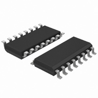
PCA9633D16,112 NXP Semiconductors, PCA9633D16,112 Datasheet - Page 14

PCA9633D16,112
Manufacturer Part Number
PCA9633D16,112
Description
IC LED DRIVER RGBA 16-SOIC
Manufacturer
NXP Semiconductors
Type
RGBA LED Driverr
Datasheet
1.PCA9633DP2118.pdf
(43 pages)
Specifications of PCA9633D16,112
Package / Case
16-SOIC (3.9mm Width)
Topology
Open Drain, PWM
Number Of Outputs
4
Internal Driver
Yes
Type - Primary
Backlight, LED Blinker
Type - Secondary
RGBA
Frequency
1MHz
Voltage - Supply
2.3 V ~ 5.5 V
Voltage - Output
5.5V
Mounting Type
Surface Mount
Operating Temperature
-40°C ~ 85°C
Current - Output / Channel
25mA
Internal Switch(s)
Yes
Low Level Output Current
17 mA
High Level Output Current
50 uA
Operating Supply Voltage
2.3 V to 5.5 V
Maximum Supply Current
100 mA
Maximum Power Dissipation
400 mW
Maximum Operating Temperature
+ 85 C
Mounting Style
SMD/SMT
Minimum Operating Temperature
- 40 C
Operating Supply Voltage (typ)
2.5/3.3/5V
Number Of Segments
8
Operating Temperature (min)
-40C
Operating Temperature (max)
85C
Operating Temperature Classification
Industrial
Package Type
SO
Pin Count
16
Mounting
Surface Mount
Power Dissipation
400mW
Operating Supply Voltage (min)
2.3V
Operating Supply Voltage (max)
5.5V
Lead Free Status / RoHS Status
Lead free / RoHS Compliant
For Use With
OM6282 - DAUGHTER CARD PCA9633 FOR OM6275OM6276,598 - DEMO BOARD PWM LED622-1004 - BOARD DEMO FOR PHILIPS PCA9633
Efficiency
-
Lead Free Status / Rohs Status
Lead free / RoHS Compliant
Other names
568-3235-5
935281309112
PCA9633D16
935281309112
PCA9633D16
NXP Semiconductors
PCA9633_5
Product data sheet
7.3.5 Group frequency, GRPFREQ
7.3.6 LED driver output state, LEDOUT
When DMBLNK bit is programmed with 1, GRPPWM and GRPFREQ registers define a
global blinking pattern, where GRPFREQ contains the blinking period (from 24 Hz to
10.73 s) and GRPPWM the duty cycle (ON/OFF ratio in %).
Table 12.
Legend: * default value.
GRPFREQ is used to program the global blinking period when DMBLNK bit (MODE2
register) is equal to 1. Value in this register is a ‘Don’t care’ when DMBLNK = 0.
Applicable to LED outputs programmed with LDRx = 11 (LEDOUT register).
Blinking period is controlled through 256 linear steps from 00h (41 ms, frequency 24 Hz)
to FFh (10.73 s).
Table 13.
Legend: * default value.
LDRx = 00 — LED driver x is off (default power-up state).
LDRx = 01 — LED driver x is fully on (individual brightness and group dimming/blinking
not controlled).
LDRx = 10 — LED driver x individual brightness can be controlled through its PWMx
register.
LDRx = 11 — LED driver x individual brightness and group dimming/blinking can be
controlled through its PWMx register and the GRPPWM registers.
duty cycle
global blinking period
Address
07h
Address
08h
GRPFREQ - Group Frequency register (address 07h) bit description
Register
GRPFREQ
LEDOUT - LED driver output state register (address 08h) bit description
Register
LEDOUT
=
GDC 7:0
-------------------------- -
256
Bit
7:0
Bit
7:6
5:4
3:2
1:0
Rev. 05 — 25 July 2008
=
GFRQ 7:0
--------------------------------------- - in
Symbol
GFRQ[7:0]
Symbol
LDR3
LDR2
LDR1
LDR0
24
+
1
Access Value
R/W
Access Value
R/W
R/W
R/W
R/W
sec
onds
0000 0000* GRPFREQ register
00*
00*
00*
00*
4-bit Fm+ I
Description
Description
LED3 output state control
LED2 output state control
LED1 output state control
LED0 output state control
PCA9633
2
© NXP B.V. 2008. All rights reserved.
C-bus LED driver
14 of 43
(2)
(3)


