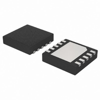
NCP5050MTTXG ON Semiconductor, NCP5050MTTXG Datasheet - Page 5

NCP5050MTTXG
Manufacturer Part Number
NCP5050MTTXG
Description
IC LED DRIVR PHOTO FLASH 10-WDFN
Manufacturer
ON Semiconductor
Type
Photo Flash LEDr
Datasheet
1.NCP5050MTTXG.pdf
(14 pages)
Specifications of NCP5050MTTXG
Constant Current
Yes
Topology
PWM, Step-Up (Boost)
Number Of Outputs
1
Internal Driver
Yes
Type - Primary
Backlight, Flash/Torch
Type - Secondary
White LED
Frequency
1.48MHz ~ 1.95MHz
Voltage - Supply
2.7 V ~ 5.5 V
Voltage - Output
20V
Mounting Type
Surface Mount
Package / Case
10-WFDFN Exposed Pad
Operating Temperature
-10°C ~ 85°C
Internal Switch(s)
Yes
Efficiency
88%
Number Of Segments
5
Operating Supply Voltage
2.7 V to 5.5 V
Maximum Operating Temperature
+ 85 C
Mounting Style
SMD/SMT
Minimum Operating Temperature
- 10 C
Lead Free Status / RoHS Status
Lead free / RoHS Compliant
Current - Output / Channel
-
Lead Free Status / Rohs Status
Details
Other names
NCP5050MTTXG
NCP5050MTTXGOSTR
NCP5050MTTXGOSTR
Available stocks
Company
Part Number
Manufacturer
Quantity
Price
Company:
Part Number:
NCP5050MTTXG
Manufacturer:
ON Semiconductor
Quantity:
1 050
Part Number:
NCP5050MTTXG
Manufacturer:
ON/安森美
Quantity:
20 000
9. Guaranteed by design and characterized
10. Efficiency is defined by 100 * (P
11. The overall tolerance is dependent on the accuracy of the external resistor. A 1% tolerance metal film resistor is recommended to achieve
12. With Schottky diode MBR130LSF and TDK VLF5014A−2R7M1R5 inductor.
ELECTRICAL CHARACTERISTICS
to 5.5 V (Unless otherwise noted). Typical values are referenced to T
Operating Power Supply
Maximum Inductor Current (Notes 9 and 11) (see Figure 24)
Refer Switch Current Limit section @ 25°C
Power Switch ON Resistor
High Current Sense Switch ON Resistor (I = 100 mA and 25°C)
Low Current Sense Switch ON Resistor (I = 100 mA and 25°C)
PWM Oscillator Frequency
Maximum Duty Cycle
Efficiency (Notes 9 and 10)
Over−voltage Clamp Voltage
Over−voltage Clamp Hysteresis
Output power (Notes 9 and 12)
Feedback Voltage Ripple Rejection @ I
Feedback Voltage in Steady State.@ T
Input Feedback Current (CM = Low)
V
Undervoltage Lockout Hysteresis
Standby Current, I
Quiescent Current, I
Startup Time (Note 9)
Inrush Peak Current Limit (Note 9)
Upper Limit of PWM Dimming Frequency (Note 9)
Time out Protection (Note 9)
Thermal Shutdown Protection (Note 9)
Thermal Shutdown Protection Hysteresis (Note 9)
Voltage Input Logic Low (Pin CM, CTRL)
Voltage Input Logic High (Pin CM, CTRL)
CTRL and CM Pin Pulldown Resistance
V
Load = 80 mA, 4 LED (V
I
in
PEAK_MAX
in
Undervoltage Lockout
= 4.2 V, L = TDK VLF5014A−2R7M1R5
T
@ V
@ V
From DC to 300 Hz (0.2 V
V
From CTRL =1.2 V to Start of Switching
Time Constant
A
in
$20 % accuracy.
= 25°C (I = 100 mA)
Decreasing
in
in
= 3.3 V
= 2.7 V
out
out
= 0 mA, CTRL = Low, V
= 0 mA, Not Switching @ T
F
Characteristics
= 3.5 V per LED, C
out
/ P
PP
) (Note 9)
A
in
out
) at 25°C
= 25°C
Minimum and Maximum Limits apply for T
= 20 mA
in
out
= 4.2 V @ T
= 1 mF X5R
A
= 25°C
http://onsemi.com
A
= 25°C
5
A
= +25°C and V
HCSSR
LCSSR
I
SWR
PEAK_MAX
Symbol
IQ
OVP
M
U
OVP
F
U
I
L
S
T
T
R
STDB
P
I
E
F
D
T
VLOH
NOSW
V
DUTY
I
PCL
V
V
OSC
REG
OUT
SDH
VLO
TRT
PLD
FB
out
BV
SD
FF
IM
IH
in
DSON
IL
ON
DSON
DSON
H
A
in
between −10°C to +85°C and V
= 3.6 V (Unless otherwise noted)
−15%
1.48
91.5
Min
215
175
2.7
1.0
4.5
2.8
5.0
2.0
1.2
85
20
−
−
−
−
−
−
−
−
−
−
−
−
−
−
Typ
200
250
750
250
100
160
250
1.7
1.0
2.5
1.2
94
90
50
20
−
−
−
−
−
−
−
−
1
−
−
−
+15%
IN
Max
1.95
0.15
285
200
375
5.5
3.0
2.7
2.0
2.0
0.4
50
−
−
−
−
−
−
−
−
−
−
−
−
−
between 2.7 V
MHz
Unit
kHz
mW
mW
mW
mV
mV
mV
mA
ms
kW
mA
mA
°C
°C
ms
%
%
W
V
A
V
V
V
V
V
s


