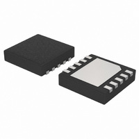
NCP5050MTTXG ON Semiconductor, NCP5050MTTXG Datasheet - Page 4

NCP5050MTTXG
Manufacturer Part Number
NCP5050MTTXG
Description
IC LED DRIVR PHOTO FLASH 10-WDFN
Manufacturer
ON Semiconductor
Type
Photo Flash LEDr
Datasheet
1.NCP5050MTTXG.pdf
(14 pages)
Specifications of NCP5050MTTXG
Constant Current
Yes
Topology
PWM, Step-Up (Boost)
Number Of Outputs
1
Internal Driver
Yes
Type - Primary
Backlight, Flash/Torch
Type - Secondary
White LED
Frequency
1.48MHz ~ 1.95MHz
Voltage - Supply
2.7 V ~ 5.5 V
Voltage - Output
20V
Mounting Type
Surface Mount
Package / Case
10-WFDFN Exposed Pad
Operating Temperature
-10°C ~ 85°C
Internal Switch(s)
Yes
Efficiency
88%
Number Of Segments
5
Operating Supply Voltage
2.7 V to 5.5 V
Maximum Operating Temperature
+ 85 C
Mounting Style
SMD/SMT
Minimum Operating Temperature
- 10 C
Lead Free Status / RoHS Status
Lead free / RoHS Compliant
Current - Output / Channel
-
Lead Free Status / Rohs Status
Details
Other names
NCP5050MTTXG
NCP5050MTTXGOSTR
NCP5050MTTXGOSTR
Available stocks
Company
Part Number
Manufacturer
Quantity
Price
Company:
Part Number:
NCP5050MTTXG
Manufacturer:
ON Semiconductor
Quantity:
1 050
Part Number:
NCP5050MTTXG
Manufacturer:
ON/安森美
Quantity:
20 000
Stresses exceeding Maximum Ratings may damage the device. Maximum Ratings are stress ratings only. Functional operation above the
Recommended Operating Conditions is not implied. Extended exposure to stresses above the Recommended Operating Conditions may affect
device reliability.
1. Maximum electrical ratings are defined as those values beyond which damage to the device may occur at T
2. According to JEDEC standard JESD22−A108B.
3. This device series contains ESD protection and passes the following tests:
4. Latch up Current Maximum Rating: $100 mA per JEDEC standard: JESD78.
5. The thermal shutdown set to 160°C (typical) avoids irreversible damage on the device due to power dissipation.
6. For the 10−Pin 3x3 WDFN Package, the R
7. Per IPC/JEDEC standard: J−STD−020A.
8. The maximum package power dissipation limit must not be exceeded.
MAXIMUM RATINGS
P
Power Supply Voltage (Note 2)
Over Voltage Protection
Human Body Model (HBM) ESD Rating (Note 3)
HCS and FB Pins
Machine Model (MM) ESD Rating (Note 3)
HCS and FB Pins
Digital Input Voltage
Digital Input Current
WDFN 3x3 Package
Power Dissipation @ T
Thermal Resistance, Junction−to−Case
Thermal Resistance, Junction−to−Air
Operating Ambient Temperature Range
Operating Junction Temperature Range
Maximum Junction Temperature
Storage Temperature Range
Moisture Sensitivity Level (Note 7)
Human Body Model (HBM) per JEDEC standard: JESD22−A114 for all pins.
Machine Model (MM) per JEDEC standard: JESD22−A115 for all pins.
board having 51 mm
d
+
125 * T
R
qJA
A
2
A
dissipation area on circuit side and board size ground plane on other side.
(Note 1)
= +85°C
Rating
qJA
is highly dependent on the PCB heat−sink area. For example, R
http://onsemi.com
4
CTRL, CM
ESD HBM
ESD MM
Symbol
T
R
R
MSL
P
JMAX
T
V
P
T
T
qJC
qJA
stg
Vin
A
S
D
J
−0.3 < V
−10 to +125
−65 to +150
−10 to +85
(Note 5)
(Note 6)
Value
in
+150
2000
1000
200
150
7.0
1.0
25
10
< V
1
qJA
bat
A
= 25°C.
+ 0.3
can be 61°C/W for 2 layers
°C/W
Unit
mA
°C
°C
°C
°C
W
V
V
V
V
V


