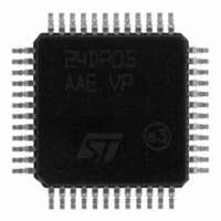
STP24DP05BTR STMicroelectronics, STP24DP05BTR Datasheet - Page 18

STP24DP05BTR
Manufacturer Part Number
STP24DP05BTR
Description
IC LED DRIVER LINEAR 48-TQFP
Manufacturer
STMicroelectronics
Type
Linear (Serial Interface)r
Datasheet
1.STP24DP05BTR.pdf
(26 pages)
Specifications of STP24DP05BTR
Constant Current
Yes
Number Of Outputs
24
Internal Driver
Yes
Type - Primary
General Purpose
Type - Secondary
RGB
Frequency
25MHz
Voltage - Supply
3 V ~ 5.5 V
Voltage - Output
20V
Mounting Type
Surface Mount
Package / Case
48-TQFP Exposed Pad, 48-eTQFP, 48-HTQFP, 48-VQFP
Operating Temperature
-40°C ~ 125°C
Current - Output / Channel
80mA
Internal Switch(s)
Yes
Low Level Output Current
- 10000 uA (Typ)
High Level Output Current
10000 uA (Typ)
Operating Supply Voltage
3.3 V to 5 V
Maximum Supply Current
40 mA
Maximum Operating Temperature
+ 125 C
Mounting Style
SMD/SMT
Minimum Operating Temperature
- 40 C
Led Driver Application
LED Displays
Topology
Constant Current
No. Of Outputs
24
Output Current
80mA
Output Voltage
20V
Input Voltage
3V To 5.5V
Operating Temperature Range
-40°C To +125°C
For Use With
497-8490 - BOARD EVAL STP24DP05/STM32 BASED
Lead Free Status / RoHS Status
Lead free / RoHS Compliant
Efficiency
-
Topology
-
Lead Free Status / Rohs Status
Lead free / RoHS Compliant
Other names
497-8283-2
Available stocks
Company
Part Number
Manufacturer
Quantity
Price
Company:
Part Number:
STP24DP05BTR
Manufacturer:
STMicroelectronics
Quantity:
10 000
Feature description
7.5
Note:
7.6
Note:
18/26
Phase three: “resuming to normal mode”
In order to re-enter in normal mode either the LE\DM pin or the sequence showed in the
following table and diagram can be used:
Table 13.
For proper device operation the “entering in detection” sequence must be followed by a
“resume mode” sequence, it is not possible to insert consecutive equal sequence.
Shift registers data flow control
The 8x3 shift registers have a default RGB sequence serial data flow as showed on block
diagram
The data can be redirected by DF0 and DF1 pins, these pins change the order of the data
flow according to the following table:
Table 14.
If the DF0 and DF1 pins are left floating, they will be pulled-up to Vdd by internal pulled-up
resistors. At such conditions the shift register sequence is set to BGR.
OE-R\DM
LE\DM
CLK
Figure 2.
Sequence
SPI sequence to resume in normal mode - truth table
Shifter register data flow control
BGR
BRG
RGB
GBR
1°
H
L
Doc ID 14714 Rev 4
2°
L
L
DF0
1
0
1
0
3°
H
L
4°
H
L
DF1
1
1
0
0
STP24DP05
5°
H
L


