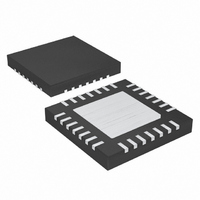
DS1864T+ Maxim Integrated Products, DS1864T+ Datasheet - Page 23

DS1864T+
Manufacturer Part Number
DS1864T+
Description
IC LASER CTRLR 1CHAN 5.5V 28TQFN
Manufacturer
Maxim Integrated Products
Type
Laser Diode Controller (Fiber Optic)r
Datasheet
1.DS1864TTR.pdf
(72 pages)
Specifications of DS1864T+
Number Of Channels
1
Voltage - Supply
2.97 V ~ 5.5 V
Current - Supply
3mA
Operating Temperature
-40°C ~ 95°C
Package / Case
28-WFQFN Exposed Pad
Mounting Type
Surface Mount
Lead Free Status / RoHS Status
Lead free / RoHS Compliant
and TX-F is set active. A falling edge of transmit disable
(the logic OR of TX-D/TXDC) will initiate a safety fault
recovery. At this point, the FETG output and the DACs
are enabled. The TX-F output will not be disabled until a
t
od to allow for system recovery. HBAL and HTXP flags
are not masked and will generate another safety fault
if their appropriate limit is exceeded. A safety fault is not
generated on standard shutdowns (the logic OR of
TX-D/TXDC).
During power-up, the device is inactive until V
exceeds the analog power-on-reset (V
time the device becomes fully functional. Once V
exceeds V
is timed to go from a 1 to a 0 and indicates when A/D
conversions begin. If V
RDYB bit reads as a 1 again. Once a device exceeds
V
active (recalled) until V
As the device powers up, the V
defaults to a 1 until the first V
and sets or clears the flag accordingly.
The DS1864 memory map is divided into seven sec-
tions that include Auxiliary Memory, Lower Memory,
and five Upper Memory tables. The Upper Memory
tables are addressed by setting the Table Select Byte
(7Fh in the Lower Memory) to the desired table number
and accessing the upper memory locations (80h to
FFh). The Lower Memory and Auxiliary Device can be
addressed at any time regardless of the state of the
Table Select Byte. The Lower Memory and Table 04h
(Table 01h in DS1859 configuration) are used to config-
ure the DS1864 and read the status of the monitors.
Memory Tables 02h and 03h contain the temperature
indexed DAC Lookup Tables. Memory Tables 05h and
01h (Table 00h in DS1859 configuration) contain masks
for alarm and warning flags. Table 01h (Table 00h in
DS1859 configuration) also contains password settings.
The Mode bit (bit 3, byte 89h in Table 04h (Table 01h in
DS1859 configuration)) selects between DS1852/
DS1856-compatible memory configuration or the
DS1859-compatible memory configuration. See Figures
16 and 17 for more information.
DS1864 has an ID hard coded in its die. Three registers
(Table 05h, bytes C0h to C2h) are assigned for this fea-
ture. Two registers are for the device ID, and a third
register is for the version number. ID registers are hard-
INITR1
POA
and the EEPROM is recalled, the values remain
Power-Up and Low-Voltage Operation
time later. LTXP is masked during this time peri-
POA
, the RDYB bit (address byte 6Eh, bit 0)
CC
CC
falls below V
ever dips below V
Memory Organization
CC
A/D conversion occurs
CC
Die Identification
____________________________________________________________________
POD
low alarm flag
POA
.
), at which
POA
, the
CC
CC
SFP Laser Controller and
wired at the time of manufacture and are globally read-
able through the I
The default DS1864 memory configuration is compati-
ble with the DS1852 memory map. The Mode bit (bit 3,
register 89h of Table 04h (Table 01h in DS1859 config-
uration)) can be selected to make the DS1864 memory
map compatible with the DS1859 memory map. Figure
16 shows the DS1852/DS1856 compatible configuration
(default), and Figure 17 shows the DS1859-compatible
configuration.
When the DS1864 is in the DS1852-compatible configu-
ration, user memory is in Table 01h. In contrast, when
the DS1864 is in the DS1859-compatible configuration
(having set Mode to 1), user memory is in Table 00h. In
addition, Table 04h in the DS1852 configuration will be
reassigned as Table 01h in the DS1859 configuration.
The memory of the DS1864 is protected by two pass-
words, PW1 (user password) and a PW2 (vendor pass-
word). The password entry location for both passwords
is in 7Bh-7Eh of Lower Memory and resides in SRAM.
The PW2 password setting locations are in Table 04h
(Table 01h in DS1859 configuration), registers C1h to
C6h. The PW1 password settings are in Table 05h, reg-
isters D1h to D6h. Password setting and password
entry bytes are write only (read as 0s).
Furthermore, the Auxiliary Memory and Main Device
Memory are divided into eight blocks; see Table 9. The
read and write protection for each block is activated by
an enable bit. Two sets of enable bytes are used for
both PW1 and PW2 level access, one byte to allow read
access to the memory blocks and one byte for write
access to the memory blocks. The two PW2 password
enable bytes are located in Table 04h (Table 01h in
DS1859 configuration), registers C1h and C2h. The
PW1 password enable bytes are located in Table 05h,
registers D1h and D2h. Table 8 shows how the pass-
word enable bytes can be configured to protect the
memory blocks. Table 9 shows the bit assignments for
each of the eight blocks of DS1864 memory. See the
registers mentioned above in the Memory Map section
for more details.
Note that regardless of read/write permissions for a
given table, password settings and password entry are
unconditionally read protected. They are write protect-
ed if the proper write enable bit is set to 1. Bytes 78h to
7Fh in Lower Memory are unprotected.
Memory Protection and Passwords
2
C interface.
Diagnostic IC
Memory Map Configurations
23


