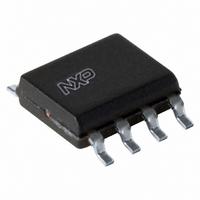
PCA9511AD,118 NXP Semiconductors, PCA9511AD,118 Datasheet - Page 13

PCA9511AD,118
Manufacturer Part Number
PCA9511AD,118
Description
IC HOTSWAP I2C/SMBUS BUFF 8SOIC
Manufacturer
NXP Semiconductors
Type
I²C-Bus and SMBus Switchr
Datasheet
1.PCA9511ADP118.pdf
(24 pages)
Specifications of PCA9511AD,118
Package / Case
8-SOIC (0.154", 3.90mm Width)
Applications
Hot-Swap/SMB Buffer
Internal Switch(s)
Yes
Current Limit
50mA
Voltage - Supply
2.7 V ~ 5.5 V
Operating Temperature
-40°C ~ 85°C
Mounting Type
Surface Mount
Supply Voltage (max)
5.5 V
Supply Voltage (min)
2.7 V
Maximum Operating Temperature
+ 85 C
Mounting Style
SMD/SMT
Minimum Operating Temperature
- 40 C
Lead Free Status / RoHS Status
Lead free / RoHS Compliant
Lead Free Status / RoHS Status
Lead free / RoHS Compliant, Lead free / RoHS Compliant
Other names
935279307118
PCA9511AD-T
PCA9511AD-T
PCA9511AD-T
PCA9511AD-T
NXP Semiconductors
Table 5.
V
[1]
[2]
[3]
[4]
[5]
[6]
[7]
[8]
PCA9511A_4
Product data sheet
Symbol
Input-output connection
V
t
t
C
V
I
System characteristics
f
t
t
t
t
t
t
t
t
t
t
PLH
PHL
LI
SCL
BUF
HD;STA
SU;STA
SU;STO
HD;DAT
SU;DAT
LOW
HIGH
f
r
CC
offset
OL
i(SCL/SDA)
= 2.7 V to 5.5 V; T
This specification applies over the full operating temperature range.
The enable time can slow considerably for some parts when temperature is < 20 C.
Delays that can occur after ENABLE and/or idle times have passed.
Guaranteed by design, not production tested.
I
Input pull-up voltage should not exceed power supply voltage in operating mode because the rise time accelerator will clamp the voltage
to the positive supply rail.
The connection circuitry always regulates its output to a higher voltage than its input. The magnitude of this offset voltage as a function
of the pull-up resistor and V
C
trt(pu)
b
= total capacitance of one bus line in pF.
varies with temperature and V
Characteristics
Parameter
offset voltage
LOW to HIGH
propagation delay
HIGH to LOW
propagation delay
SCL and SDA input
capacitance
LOW-level output
voltage
input leakage current
SCL clock frequency
bus free time between a
STOP and START
condition
hold time (repeated)
START condition
set-up time for a
repeated
START condition
set-up time for
STOP condition
data hold time
data set-up time
LOW period of the
SCL clock
HIGH period of the
SCL clock
fall time of both SDA and
SCL signals
rise time of both SDA
and SCL signals
amb
= 40 C to +85 V; unless otherwise specified.
…continued
CC
voltage is shown in
CC
voltage, as shown in
Conditions
10 k to V
V
SCL to SCL and SDA to SDA;
10 k to V
C
SCL to SCL and SDA to SDA;
10 k to V
C
V
I
SDAn, SCLn pins; V
sink
CC
I
L
L
= 0 V; SDAn, SCLn pins;
= 100 pF each side
= 100 pF each side
= 3 mA; V
= 3.3 V
Section 11.1 “Typical performance
Rev. 04 — 19 August 2009
CC
CC
CC
;
;
on SDA, SCL;
CC
= 2.7 V
Section 11.1 “Typical performance
CC
= 5.5 V
Hot swappable I
[1][7][9]
[4][8]
[4][8]
[4]
[1]
[4]
[4]
[4]
[4]
[4]
[4]
[4]
[4]
[4]
characteristics”.
Min
0
-
-
-
0
0
1.3
0.6
0.6
0.6
300
100
1.3
0.6
20 + 0.1
20 + 0.1
1
characteristics”.
2
C-bus and SMBus bus buffer
C
C
b
b
Typ
110
0
70
5
-
-
-
-
-
-
-
-
-
-
-
-
-
PCA9511A
© NXP B.V. 2009. All rights reserved.
Max
175
-
-
7
0.4
+1
400
-
-
-
-
-
-
-
-
300
300
13 of 24
Unit
mV
ns
ns
pF
V
kHz
ns
ns
ns
ns
A
s
s
s
s
s
s


