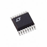
LTC1642IGN Linear Technology, LTC1642IGN Datasheet - Page 9

LTC1642IGN
Manufacturer Part Number
LTC1642IGN
Description
IC CONTROLLER HOTSWAP ADJ 16SSOP
Manufacturer
Linear Technology
Type
Hot-Swap Controllerr
Specifications of LTC1642IGN
Applications
General Purpose, Infiniband™
Internal Switch(s)
No
Voltage - Supply
2.97 V ~ 16.5 V
Operating Temperature
-40°C ~ 85°C
Mounting Type
Surface Mount
Package / Case
16-SSOP (0.150", 3.90mm Width)
Lead Free Status / RoHS Status
Contains lead / RoHS non-compliant
APPLICATIO S I FOR ATIO
Hot Circuit Insertion
When a circuit board is inserted into a live backplane its
supply bypass capacitors can draw large currents from the
backplane power bus as they charge. These currents can
permanently damage connector pins and can glitch the
backplane supply, resetting other boards in the system.
The LTC1642 limits the charging currents drawn by a
board’s capacitors, allowing safe insertion into a live
backplane.
In the circuit shown in Figure 1 the LTC1642 and the
external NMOS pass transistor Q1 work together to limit
charging currents. Waveforms at board insertion are
shown in Figure 2. When power is first applied to V
chip holds Q1’s gate at ground. After an adjustable delay
a 25µA current source begins to charge the external
capacitor C2, so choose C2 to limit the inrush current
I
according to the equation:
An internal charge pump supplies the 25µA gate current,
ensuring sufficient gate drive to Q1. At 3V V
gate drive is 4.5V; at 5V V
the minimum is again 4.5V, due to an internal zener clamp
from the GATE pin to ground. Resistor R3 limits this zener’s
transient current during board insertion and removal and
protects against high frequency oscillations in Q1. D1
provides additional protection against supply spikes.
INRUSH
0.33µF
2.5A
12V
V
C2 C
IN
C4
=
charging the board’s bypass capacitance C
R7
24k
R10
30k
LOAD
0.33µF
4
2
Figure 1. Supply Control Circuitry
C1
ON
BRK TMR
RST TMR
•
V
I
INRUSH
CC
25 A
LTC1642
0.010Ω
16
3
U
R2
µ
SENSE
CC
FAULT
GATE
15
GND
U
the minimum is 10V; at 15V V
8
1642 F01
14
6
FDS6630A
ALL RESISTORS ±5% UNLESS NOTED
RESET DELAY = 200ms
SHORT-CIRCUIT DURATION = 10ms
Q1
R3
100Ω
R4
330Ω
W
C2
0.047µF
+
CC
C
the minimum
LOAD
D1
1N4705
18V
V
U
OUT
CC
LOAD
the
CC
The delay before the GATE pin voltage begins ramping is
determined by the system timer. It comprises an external
capacitor C1 from the RST TMR pin to ground; an internal
2µA current source feeding RST TMR from V
comparator, with the noninverting input tied to RST TMR
and the inverting input tied to the 1.22V reference; and an
internal NMOS pull-down. In standby, the NMOS holds
RST TMR at ground. When the timer starts the NMOS
turns off and the RST TMR voltage ramps up as the current
source charges the capacitor. When RST TMR reaches
1.22V the timer comparator trips, the GATE voltage begins
ramping up and RST TMR returns to ground. The timer
delay is:
The second RST TMR cycle indicates that V
tolerance; it is discussed in the Undervoltage Monitor
section.
Powering-Up in Current Limit
Ramping the GATE pin voltage limits the current to I =
25µA • C
connected to the GATE and C
If the value of C
can often result in needlessly long ramp times, and it may
be better to limit the charging current by powering up in
current limit.
Current Limiting and Solid-State Circuit Breaker
The current can be limited by connecting a sense resistor
between the LTC1642’s V
voltage drop across this resistor reaches a limiting value,
t
RSTTMR
RST TMR
10V/DIV
20V/DIV
20V/DIV
2V/DIV
GATE
V
OUT
OV
LOAD
= (615ms/µF) C1.
Figure 2. Timing at Board Insertion
/C2, where C2 is the external capacitor
LOAD
is uncertain, then a worst-case design
CC
100ms/DIV
LOAD
and SENSE pins. When the
is the load capacitance.
LTC1642
CC
OUT
; an internal
1642 F02
is within
1642fb
9


