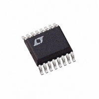
LTC1642IGN Linear Technology, LTC1642IGN Datasheet - Page 6

LTC1642IGN
Manufacturer Part Number
LTC1642IGN
Description
IC CONTROLLER HOTSWAP ADJ 16SSOP
Manufacturer
Linear Technology
Type
Hot-Swap Controllerr
Specifications of LTC1642IGN
Applications
General Purpose, Infiniband™
Internal Switch(s)
No
Voltage - Supply
2.97 V ~ 16.5 V
Operating Temperature
-40°C ~ 85°C
Mounting Type
Surface Mount
Package / Case
16-SSOP (0.150", 3.90mm Width)
Lead Free Status / RoHS Status
Contains lead / RoHS non-compliant
LTC1642
CRWBR (Pin 1): Overvoltage Crowbar Circuit Timer and
Trigger. This pin controls an external overvoltage crowbar
circuit. A capacitor from the pin to ground sets a 9ms/µF
delay after an overvoltage occurs until an external SCR is
triggered. See Applications Information. Ground the
CRWBR pin if unused.
BRK TMR (Pin 2): Circuit Breaker Timer. Connect a
capacitor from BRK TMR to ground to set a 60ms/µF delay
from the time the sense resistor current reaches its limit
until the FET is shut off. FAULT output is then asserted and
the FET remains off until the chip is reset. Ground BRK
TMR to allow the part to remain in current limit indefinitely.
RST TMR (Pin 3): Analog System/Reset Timer. A capaci-
tor from this pin to ground sets a 0.6s/µF delay from the
ON pin going high to the start of the GATE pin’s ramp. It
also sets the delay from output voltage good, as sensed by
the FB pin, to RESET going high.
ON (Pin 4): ON Control Input. When ON is low the GATE
pin is grounded and FAULT goes high. The GATE pin
voltage starts ramping up one RST TMR timing cycle after
ON goes high. Pulsing the ON pin low for at least 2µs resets
the chip if it latches off after a sustained overvoltage or
current limit. The threshold for a low to high transition is
1.34V with 110mV of hysteresis. A 21V zener clamp limits
the voltage at this pin. The pin can be safely tied to V
21V through a series resistor that limits the current below
1mA.
PI FU CTIO S
6
U
U
U
CC
>
RESET (Pin 5): Open Drain Reset Output. RESET is pulled
low if the voltage at the FB pin is below its trip point. RESET
goes high one RESET timing cycle after the FB voltage
exceeds its trip point plus 3mV of hysteresis. RESET has
a weak pull-up to one diode drop below V
resistor can pull the pin above V
limits the voltage at this pin. The pin can be safely tied to
V
below 1mA.
FAULT (Pin 6): Open Drain Fault Output. FAULT is pulled
low when the part turns off following a sustained overvolt-
age or current limit. It goes high 2µs after the ON pin goes
low. FAULT has a weak pull-up to one diode drop below
V
21V zener clamp limits the voltage at this pin. The pin can
be safely tied to V
limits the current below 1mA.
FB (Pin 7): Output Voltage Monitor and Foldback Input.
The FB comparator can be used with an external resistive
divider to monitor the output supply voltage. When the FB
voltage is lower than 1.22V the RESET pin is pulled low.
RESET goes high one system timing cycle after the voltage
at FB exceeds its threshold by 3mV of hysteresis. A low
pass filter at the comparator’s output prevents negative
voltage glitches from triggering a false reset.
GND (Pin 8): Chip Ground.
CC
CC
> 21V through a series resistor that limits the current
and an external resistor can pull the pin above V
CC
> 21V through a series resistor that
CC
. A 21V zener clamp
CC
and an external
CC
1642fb
. A


