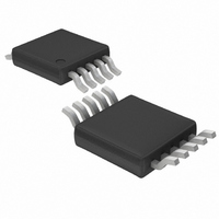
LTC4252A-2IMS#TRPBF Linear Technology, LTC4252A-2IMS#TRPBF Datasheet - Page 15

LTC4252A-2IMS#TRPBF
Manufacturer Part Number
LTC4252A-2IMS#TRPBF
Description
IC CNTRLR HOTSWAP NEGVOLT 10MSOP
Manufacturer
Linear Technology
Type
Hot-Swap Controllerr
Datasheet
1.LTC4252-1CMS8PBF.pdf
(36 pages)
Specifications of LTC4252A-2IMS#TRPBF
Applications
General Purpose
Internal Switch(s)
No
Operating Temperature
-40°C ~ 85°C
Mounting Type
Surface Mount
Package / Case
10-TFSOP, 10-MSOP (0.118", 3.00mm Width)
Lead Free Status / RoHS Status
Lead free / RoHS Compliant
Available stocks
Company
Part Number
Manufacturer
Quantity
Price
APPLICATIONS INFORMATION
and R2 = 32.4k gives a typical operating range of 43.2V
to 82.5V. The undervoltage shutdown and overvoltage
recovery thresholds are then 39.2V and 74.4V. 1% divider
resistors are recommended to preserve threshold accuracy.
The R1-R2 divider values shown in the Typical Application
set a standing current of slightly more than 100μA and
define an impedance at UV/OV of 30kΩ. In most applica-
tions, 30kΩ impedance coupled with 300mV UV hysteresis
makes the LTC4252 insensitive to noise. If more noise
immunity is desired, add a 1nF to 10nF filter capacitor
from UV/OV to V
Separate UV and OV pins are available in the 10-pin MS
package and can be used for a different operating range
such as 35.5V to 76V as shown in Figure 3. Other combi-
nations are possible with different resistor arrangements.
UV/OV COMPARATORS (LTC4252A)
A UV hysteretic comparator detects undervoltage condi-
tions at the UV pin, with the following thresholds:
An OV hysteretic comparator detects overvoltage condi-
tions at the OV pin, with the following thresholds:
UV low-to-high (V
UV high-to-low (V
EE
.
(SHORT PIN)
UV
UV
–48RTN
–48RTN
) = 3.08V
– V
–48V
UVHST
* M0C207
Q2: MMBT5551LT1
464k
10k
34k
Figure 4. – 48V/2.5A Application with Wider Input Operating Range
1%
1%
1%
R1
R2
R3
) = 2.756V
C2
10nF
**DIODES, INC
†
C
0.68μF
RECOMMENDED FOR HARSH ENVIRONMENTS
T
10
9
8
3
OV
TIMER
UV
SS
C
68nF
SS
LTC4252A-1
V
V
EE
IN
5
1
R
10k
1/2W
IN
The UV and OV trip point ratio is designed to match the
standard telecom operating range of 43V to 71V when
connected together as in Figure 2. A divider (R1, R2) is
used to scale the supply voltage. Using R1 = 390k and R2
= 30.1k gives a typical operating range of 43V to 71V. The
undervoltage shutdown and overvoltage recovery thresh-
olds are then 38.5V and 69.6V respectively. 1% divider
resistors are recommended to preserve threshold accuracy.
The R1-R2 divider values shown in Figure 2 set a standing
current of slightly more than 100μA and define an impedance
at UV/OV of 28kΩ. In most applications, 28kΩ impedance
coupled with 324mV UV hysteresis makes the LTC4252A
insensitive to noise. If more noise immunity is desired, add
a 1nF to 10nF filter capacitor from UV/OV to V
The UV and OV pins can be used for a wider operat-
ing range such as 35.5V to 76V as shown in Figure 4.
Other combinations are possible with different resistor
arrangements.
UV/OV OPERATION
A low input to the UV comparator will reset the chip and pull
the GATE and TIMER pins low. A low-to-high UV transition
will initiate an initial timing sequence if the other interlock
PWRGD
SENSE
DRAIN
GATE
OV low-to-high (V
OV high-to-low (V
D
DDZ13B
IN
†
LTC4252A-1/LTC4252A-2
2
7
6
4
**
LTC4252-1/LTC4252-2
22k
C
1μF
R4
IN
R
D
1M
Q2
OV
OV
R5
2.2k
R
10Ω
) = 5.09V
C
– V
C
10nF
100μF
C
*
425212 F04
C
OVHST
L
+
Q1
IRF530S
R
0.02Ω
S
EN
) = 4.988V
LOAD
EE
.
15
425212fc


