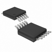
LTC4212CMS Linear Technology, LTC4212CMS Datasheet - Page 8

LTC4212CMS
Manufacturer Part Number
LTC4212CMS
Description
IC CTRLR HOTSWAP TIMEOUT 10MSOP
Manufacturer
Linear Technology
Type
Hot-Swap Controllerr
Datasheet
1.LTC4212CMS.pdf
(24 pages)
Specifications of LTC4212CMS
Applications
General Purpose
Internal Switch(s)
No
Voltage - Supply
2.5 V ~ 16.5 V
Operating Temperature
0°C ~ 70°C
Mounting Type
Surface Mount
Package / Case
10-TFSOP, 10-MSOP (0.118", 3.00mm Width)
Lead Free Status / RoHS Status
Contains lead / RoHS non-compliant
Available stocks
Company
Part Number
Manufacturer
Quantity
Price
Company:
Part Number:
LTC4212CMS
Manufacturer:
LT
Quantity:
10 000
PI FU CTIO S
LTC4212
ON (Pin 1): On/Off Control Input. The ON pin is used to
enable and disable LTC4212 operation and reset internal
logic and the electronic circuit breaker (ECB). It must be
pulled high (>1.316V) to start the first system timing
cycle. If the ON pin is pulled low (<0.455V typical) for more
than 10 s, the internal logic is reset and the GATE pin is
pulled down by a 200 A current to turn off the external
FET. If the ON pin is pulled low for more than 120 s, the
electronic circuit breaker is reset. This pin is tied to a
resistive divider in latch-off applications or to the FAULT
pin and an external RC circuit in auto-retry applications.
TIMER (Pin 2): System Timer Input. An external capacitor
(C
the duration of the first and second system timing cycles.
The first timing cycle allows time for the board to be
inserted properly. During the second timing cycle, a
soft-start circuit controls the gate of the external
N-channel FET to limit inrush currents from the backplane
supply.
PGT (Pin 3): Power Good Timer Input. An external capaci-
tor (C
power good time-out period. This is the maximum time
allowed for externally monitored DC/DC converters to
power-up into regulation and pull the PGI pin high. The
nominal time-out cycle is 1.81s/ F and begins from the
end of the second system timing cycle. This pin is pulled
to ground by an internal switch when the power good timer
is disabled or when the ECB is tripped.
PGF (Pin 4): Power Good Glitch Filter Input. An external
capacitor (C
mines the power good glitch filter delay. The glitch filter is
enabled if the externally monitored DC/DC converters are
powered up within the power good time-out period (see
Pin 3). If the PGI pin goes low for longer than the filter
delay, the ECB is tripped.
GND (Pin 5): Device Ground Connection. Connect this pin
to the system’s analog ground plane.
PGI (Pin 6): Power Good Input Pin. This pin is used by the
power good circuit to sense the open drain RST output or
comparator outputs of an external supply monitor IC or
the PGOOD output of a DC/DC converter. It requires an
external pull-up resistor to a voltage above the V
8
TIMER
U
PGT
) connected from this pin to ground determines
) connected from this pin to ground sets the
U
PGF
) connected from this pin to ground deter-
U
FAULT
threshold 1.236V. When the power good timer times out
(see Pin 3), PGI must be high to avoid tripping the ECB and
to enable the power good glitch filter.
GATE (Pin 7): Gate Output Pin. The output signal at this
pin is the high side gate drive for the external N-channel
FET pass transistor.
As shown in the Block Diagram, an internal charge pump
supplies a 10 A gate current and sufficient gate voltage to
drive the external FET for supply voltages from 2.5V to
16.5V. The internal charge pump and zener clamps at the
charge pump output determine the gate drive voltage
( V
minimum 4V of V
V
zener clamp Z1 connected between the charge pump
output and the V
with guaranteed minimum value of 10V. For V
zener clamp Z2 sets the limitation for V
the gate voltage to ground to 28V typically. The minimum
Z2’s clamp voltage is 23V. This effectively sets V
8V minimum.
SENSE (Pin 8): Circuit Breaker Set Pin. With a sense
resistor placed in the power path between V
the LTC4212’s electronic circuit breaker trips if the voltage
across the sense resistor exceeds the thresholds set
internally for the SLOW COMP and the FAST COMP, as
shown in the Block Diagram. The threshold for the SLOW
COMP is V
breaker trips if the voltage across the sense resistor
exceeds 50mV for 18 s.
Under transient conditions where large step current
changes can and do occur over shorter periods of time, a
second (fast) comparator instead trips the electronic
circuit breaker. The threshold for the FAST COMP is set at
V
voltage across the sense resistor exceeds 150mV for more
than 500ns. To disable the electronic circuit breaker,
connect the V
V
LTC4212 operates from 2.5V < V
current is typically 1mA. An internal undervoltage lockout circuit
disables the device until the voltage at V
CC
CC
CB(FAST)
GATE
(Pin 9): This is the positive supply input to the LTC4212. The
< 4.75V. For V
= V
= 150mV, and the circuit breaker trips if the
CB(SLOW)
GATE
CC
CC
and SENSE pins together.
– V
GATE
pin. The V
CC
= 50mV, and the electronic circuit
CC
> 4.75V, the V
for supplies in the range of 2.5V <
). The charge pump produces a
GATE
CC
< 16.5V, and the supply
is typically at 12V and
CC
GATE
exceeds 2.34V.
GATE
CC
is limited by
CC
and SENSE,
. Z2 clamps
> 15V, the
GATE
4212f
to


