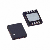
LTC4300A-3CDD Linear Technology, LTC4300A-3CDD Datasheet - Page 8

LTC4300A-3CDD
Manufacturer Part Number
LTC4300A-3CDD
Description
IC BUFFER BUS HOTSWAP 2WR 8DFN
Manufacturer
Linear Technology
Type
Hot-Swap Switchr
Datasheet
1.LTC4300A-3CMS8.pdf
(12 pages)
Specifications of LTC4300A-3CDD
Applications
General Purpose, Buffer/Bus Extender
Internal Switch(s)
Yes
Voltage - Supply
2.7 V ~ 5.5 V
Operating Temperature
0°C ~ 70°C
Mounting Type
Surface Mount
Package / Case
8-WFDFN Exposed Pad
Lead Free Status / RoHS Status
Contains lead / RoHS non-compliant
Available stocks
Company
Part Number
Manufacturer
Quantity
Price
Company:
Part Number:
LTC4300A-3CDD
Manufacturer:
LT
Quantity:
10 000
LTC4300A-3
OPERATIO
temperature and the pull-up resistors and equivalent bus
capacitances on both sides of the bus. The Typical Perfor-
mance Characteristics section shows t
temperature and voltage for 10k pull-up resistors and
100pF equivalent capacitance on both sides of the part. By
comparison with Figure 2, the V
shows that increasing the capacitance from 50pF to 100pF
results in a propagation delay increase from 55ns to 75ns.
Larger output capacitances translate to longer delays (up
to 150ns). Users must quantify the difference in propaga-
tion times for a rising edge versus a falling edge in their
systems and adjust setup and hold times accordingly.
Rise-Time Accelerators
Once connection has been established, rise-time accelera-
tor circuits on all four SDA and SCL pins are activated.
These allow the user to choose weaker DC pull-up currents
on the bus, reducing power consumption while still meet-
ing system rise-time requirements. During positive bus
transitions, the LTC4300A-3 switches in 2mA (typical) of
current to quickly slew the SDA and SCL lines once their
DC voltages exceed 0.6V. Using a general rule of 20pF of
capacitance for every device on the bus (10pF for the
device and 10pF for interconnect), choose a pull-up cur-
rent so that the bus will rise on its own at a rate of at least
1.25V/µs to guarantee activation of the accelerators.
8
Figure 1. Input–Output Connection Low to High Transition
0.5V/DIV
OUTPUT
SIDE
50pF
U
200ns/DIV
CC
= V
PHL
4300A-3 F01
CC2
as a function of
= 3.3V curve
INPUT
SIDE
150pF
For example, assume an SMBus system with V
10k pull-up resistor and equivalent bus capacitance of
200pF. The rise-time of an SMBus system is calculated
from (V
2.25V. It takes an RC circuit 0.92 time constants to
traverse this voltage for a 3V supply; in this case, 0.92 •
(10k • 200pF) = 1.84µs. Thus, the system exceeds the
maximum allowed rise-time of 1µs by 84%. However,
using the rise-time accelerators, which are activated at a
DC threshold of below 0.65V, the worst-case rise-time is:
(2.25V – 0.65V) • 200pF/1mA = 320ns, which meets the
1µs rise-time requirement.
ENABLE Low Current Disable
Grounding the ENABLE pin disconnects the backplane
side from the card side, disables the rise-time accelera-
tors, disables the bus precharge circuitry and puts the part
in a near-zero current state. When the pin voltage is driven
all the way to V
both the backplane and card sides to be complete (as
described in the Start-Up section) before reconnecting the
two sides.
Figure 2. Input–Output Connection High to Low Transition
0.5V/DIV
IL(MAX)
INPUT
150pF
SIDE
– 0.15V) to (V
CC
, the part waits for data transactions on
200ns/DIV
IH(MIN)
+ 0.15V), or 0.65V to
4300A-3 F02
OUTPUT
SIDE
50pF
sn4300a3 4300a3fs
CC
= 3V, a


