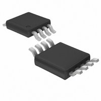
LTC4300-2CMS8 Linear Technology, LTC4300-2CMS8 Datasheet - Page 5

LTC4300-2CMS8
Manufacturer Part Number
LTC4300-2CMS8
Description
IC HOT SWAP 2WIRE BUS BUFR MSOP8
Manufacturer
Linear Technology
Type
Hot-Swap Switchr
Datasheet
1.LTC4300-1CMS8.pdf
(16 pages)
Specifications of LTC4300-2CMS8
Applications
General Purpose, Buffer/Bus Extender
Internal Switch(s)
Yes
Voltage - Supply
2.7 V ~ 5.5 V
Operating Temperature
0°C ~ 70°C
Mounting Type
Surface Mount
Package / Case
8-TSSOP, 8-MSOP (0.118", 3.00mm Width)
Lead Free Status / RoHS Status
Contains lead / RoHS non-compliant
Other names
Q1354742
Available stocks
Company
Part Number
Manufacturer
Quantity
Price
Part Number:
LTC4300-2CMS8
Manufacturer:
LT/凌特
Quantity:
20 000
Company:
Part Number:
LTC4300-2CMS8#TRPBF
Manufacturer:
TI
Quantity:
4 516
Part Number:
LTC4300-2CMS8#TRPBF
Manufacturer:
LT/凌特
Quantity:
20 000
PI FU CTIO S
ENABLE/V
age. For the LTC4300-1, this is a digital CMOS threshold
input pin. Grounding this pin puts the part in a low current
(<1 A) mode. It also disables the rise-time accelerators,
disables the bus precharge circuitry, drives READY low,
isolates SDAIN from SDAOUT and isolates SCLIN from
SCLOUT. Drive ENABLE all the way to V
operation. Connect ENABLE to V
being used. For the LTC4300-2, this is the supply voltage
for the devices on the card I
resistors from SDAOUT and SCLOUT to this pin. Place a
bypass capacitor of at least 0.01 F close to this pin for best
results.
SCLOUT (Pin 2): Serial Clock Output. Connect this pin to
the SCL bus on the card. See Figures 3 and 4 for bus pull-
up resistance and capacitance requirements.
SCLIN (Pin 3): Serial Clock Input. Connect this pin to the
SCL bus on the backplane. See Figures 3 and 4 for bus pull-
up resistance and capacitance requirements.
GND (Pin 4): Ground. Connect this pin to a ground plane
for best results.
U
CC2
U
(Pin 1): Chip Enable Pin/Card Supply Volt-
U
2
C busses. Connect pull-up
CC
if this feature is not
CC
for normal
READY/ACC (Pin 5): Connection Flag/Rise-Time Accel-
erator Control. For the LTC4300-1, this is an open-drain
NMOS output which pulls low when either ENABLE is low
or the start-up sequence described in the Operation sec-
tion has not been completed. READY goes high when
ENABLE is high and start-up is complete. Connect a 10k
resistor from this pin to V
LTC4300-2, this is a CMOS threshold digital input pin that
enables and disables the rise-time accelerators on all four
SDA and SCL pins. Drive ACC all the way to the V
voltage to enable all four accelerators; drive ACC to ground
to turn them off.
SDAIN (Pin 6): Serial Data Input. Connect this pin to the
SDA bus on the backplane. See Figures 3 and 4 for bus
pull-up resistance and capacitance requirements.
SDAOUT (Pin 7): Serial Data Output. Connect this pin to
the SDA bus on the card. See Figures 3 and 4 for bus pull-
up resistance and capacitance requirements.
V
This is the supply voltage for the devices on the backplane
I
SCLIN to this pin. Place a bypass capacitor of at least
0.01 F close to this pin for best results.
2
CC
C busses. Connect pull-up resistors from SDAIN and
(Pin 8): Main Input Power Supply from Backplane.
LTC4300-1/LTC4300-2
CC
to provide the pull up. For the
sn430012 430012fs
CC2
supply
5


