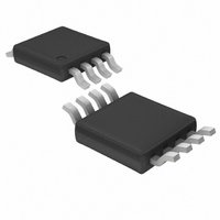
LTC4300-1IMS8#PBF Linear Technology, LTC4300-1IMS8#PBF Datasheet

LTC4300-1IMS8#PBF
Specifications of LTC4300-1IMS8#PBF
Available stocks
Related parts for LTC4300-1IMS8#PBF
LTC4300-1IMS8#PBF Summary of contents
Page 1
... The LTC4300-2 also replaces the READY pin with a digital CMOS input pin, ACC, which enables and disables the rise-time accelerator currents. The LTC4300 is available in a small 8-pin MSOP package 24k ...
Page 2
... CC2 SDAIN, SCLIN, SDAOUT, SCLOUT ................. – 0 READY, ENABLE (LTC4300-1) ....................... – 0 ACC (LTC4300-2) .......................................... – 0 Operating Temperature Range LTC4300-1C/LTC4300-2C ....................... LTC4300-1I/LTC4300-2I .................... – Storage Temperature Range ................. – 125 C Lead Temperature (Soldering, 10 sec).................. 300 C ELECTRICAL CHARACTERISTICS temperature range, otherwise specfications are at T SYMBOL PARAMETER Power Supply ...
Page 3
... The denotes the specifications which apply over the full operating = 2.7V to 5.5V, unless otherwise noted CONDITIONS Positive Transition on SDA,SCL 2.7V, CC Slew Rate = 1.25V/ s (Note 2), LTC4300-2, ACC = 0.7 • 2.7V CC2 CC2 LTC4300-2 LTC4300-2 LTC4300-2 LTC4300-2 10k SDA, SCL 3.3V (Note 3), ...
Page 4
... LTC4300-1/LTC4300 TYPICAL PERFOR A CE CHARACTERISTICS I vs Temperature (LTC4300-1) CC 3.0 2 5.5V CC 2.8 2.7 2.6 2 2.7V CC 2.4 2.3 2.2 –50 – TEMPERATURE ( Temperature PULLUPAC 2. –50 – TEMPERATURE ( 100 4300-1/2 G01 75 100 4300-1/2 G03 Input – Output t vs Temperature PHL (LTC4300-1) 100 3.3V ...
Page 5
... ENABLE/V (Pin 1): Chip Enable Pin/Card Supply Volt- CC2 age. For the LTC4300-1, this is a digital CMOS threshold input pin. Grounding this pin puts the part in a low current (<1 A) mode. It also disables the rise-time accelerators, disables the bus precharge circuitry, drives READY low, isolates SDAIN from SDAOUT and isolates SCLIN from SCLOUT ...
Page 6
... LTC4300-1/LTC4300-2 W BLOCK DIAGRA (LTC4300-1) SLEW RATE DECTECTOR SDAIN 6 CONNECT SLEW RATE DECTECTOR SCLIN 3 CONNECT + – + 0.55V / – CC 0.45V CC UVLO 95 s DELAY ENABLE 2-Wire Bus Buffer and Hot Swap Controller 2mA 2mA BACKPLANE-TO-CARD CONNECTION CONNECT ENABLE 100k RCH1 1V PRECHARGE 100k RCH2 2mA ...
Page 7
... Bus Buffer and Hot Swap Controller 2mA 2mA BACKPLANE-TO-CARD CONNECTION CONNECT 100k RCH1 1V PRECHARGE 100k RCH2 2mA 2mA BACKPLANE-TO-CARD CONNECTION STOP BIT AND BUS IDLE 0.5 A 20pF 0.5pF LTC4300-1/LTC4300-2 SLEW RATE DECTECTOR CONNECT 100k RCH3 100k RCH4 SLEW RATE DECTECTOR + CONNECT – + – CONNECT CONNECT 4300-2 BD ...
Page 8
... I/O card. Once the LTC4300 comes out of UVLO, it assumes that SDAIN and SCLIN have been hot swapped into a live system and that SDAOUT and SCLOUT are being powered up at the same time as itself ...
Page 9
... These allow the user to choose weaker DC pull-up currents on the bus, reducing power consumption while still meet- ing system rise-time requirements. During positive bus transitions, the LTC4300 switches in 2mA of current to quickly slew the SDA and SCL lines once their DC voltages exceed 0.6V. Using a general rule of 20pF of capacitance ...
Page 10
... Placing a LTC4300 on the edge of each card, however, isolates the card capacitance from the backplane. For a given I/O card, the LTC4300 drives the capacitance of everything on the card and the backplane must drive only the capacitance of the LTC4300, which is less than 10pF ...
Page 11
... ENABLE product of 10ms provides a filter to prevent the LTC4300-1 from becoming activated until the transients associated with hot swapping have settled. Figure 8 shows the LTC4300 application where the user has a custom connector with pins of three different lengths available. Making V the shortest pin ensures ...
Page 12
... 10k 10k BD_SEL SDA SCL NOTE: APPLICATION ASSUMES BUS CAPACITANCES WITHIN “PROPER OPERATION” REGION OF FIGURES 3 AND 4 Figure 5. Hot Swapping Multiple I/O Cards into a Backplane Using the LTC4300 CompactPCI System POWER SUPPLY HOT SWAP ENABLE SDAIN SCLIN POWER SUPPLY HOT SWAP ...
Page 13
... CC2 BD_SEL V CC SDA SCL R1 R2 10k 10k NOTE: APPLICATION ASSUMES BUS CAPACITANCES WITHIN “PROPER OPERATION” REGION OF FIGURES 3 AND 4 Figure 6. Hot Swapping Multiple I/O Cards into a Backplane Using the LTC4300 CompactPCI System W U POWER SUPPLY HOT SWAP 5 SDAIN SCLIN C2 0.01 F ...
Page 14
... CC2 R1 R2 10k 10k V CC SDA SCL NOTE: APPLICATION ASSUMES BUS CAPACITANCES WITHIN “PROPER OPERATION” REGION OF FIGURES 3 AND 4 Figure 8. Hot Swapping Multiple I/O Cards into a Backplane Using the LTC4300-2 with a Custom Connector I/O PERIPHERAL CARD 1 R3 100k ENABLE LTC4300-1 SDAIN SCLIN C2 0 ...
Page 15
... TYP 0.53 0.015 1.10 (.021 .006) (.043) DETAIL “A” MAX SEATING PLANE 0.22 – 0.38 (.009 – .015) LTC4300-1/LTC4300-2 2-WIRE SYSTEM 0. LTC4300-1 10k 10k V CC ENABLE SDAOUT SCLOUT SDAIN SDA1 SCLIN READY SCL1 GND 0.52 (.206 REF 3.00 0.102 ( ...
Page 16
... Voltages 0.01 F 0.01 F 10k CC2 SDAIN SDAOUT LTC4300-2 SCLIN SCLOUT U1 ACC GND Figure 11 3.3V Level Translator COMMENTS Low Single-Ended/70 Differential, ON Expandable to 32 Single or 16 Differential Channels Precision 50 A 2.5% Tolerance Over Temperature, 4 Selectable SMBus Addresses, DAC Powers up at Zero or Midscale 8 Selectable Addresses/16-Channel Capability DNL < ...


