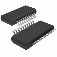
LTC4241CGN#PBF Linear Technology, LTC4241CGN#PBF Datasheet - Page 7

LTC4241CGN#PBF
Manufacturer Part Number
LTC4241CGN#PBF
Description
IC CTRLR HOTSWAP CPCI I2C 20SSOP
Manufacturer
Linear Technology
Type
Hot-Swap Controllerr
Datasheet
1.LTC4241CGN.pdf
(16 pages)
Specifications of LTC4241CGN#PBF
Applications
PCI, PCI-X
Internal Switch(s)
No
Voltage - Supply
3.3V, 5V, ±12V
Operating Temperature
0°C ~ 70°C
Mounting Type
Surface Mount
Package / Case
20-SSOP (0.154", 3.91mm Width)
Input Voltage
12V
Output Voltage
14V
Internal Switch
No
Supply Voltage Range
3.3V To 12V
Digital Ic Case Style
SSOP
No. Of Pins
20
Rohs Compliant
Yes
Lead Free Status / RoHS Status
Lead free / RoHS Compliant
Available stocks
Company
Part Number
Manufacturer
Quantity
Price
PI FU CTIO S
12V
primary controller internal circuitry. A 0.5
connected between 12V
current limit. An undervoltage lockout circuit prevents the
switches from turning on while the 12V
less than 9V.
V
connected between V
current limit.
3V
3.3V output supply voltage. The PWRGD signal cannot go
low until the 3V
TIMER (Pin 4): Current Limit Fault Timer Input. Connect a
capacitor from TIMER to ground. With the primary con-
troller turned off (ON = GND) or the internal circuit breaker
tripped due to a PCI supply fault (FAULT = low), the TIMER
pin is internally held at ground. When the primary control-
ler is turned on, a 22 A pull-up current source is con-
nected to TIMER. Current limit faults from the PCI supplies
will be ignored until the voltage at the TIMER pin rises to
within 0.9V of 12V
ON (Pin 5): On Control Input. A rising edge turns on the
external N-channel FETs for 3.3V and 5V PCI supplies, the
internal 12V and –12V switches and a falling edge turns it
off. If the ON pin is cycled low then high following the trip
of the circuit breaker due to a PCI supply fault, the circuit
breaker is reset.
FAULT (Pin 6): Fault Output. Open drain logic output used
by both the primary and auxiliary controller to indicate an
overcurrent fault condition. When any of the PCI and 3.3V
auxiliary supplies are in current limit fault, the controller
detecting the fault (primary or auxiliary) will be latched off
and the FAULT pin will be pulled low. Current limit faults
from the PCI supplies are ignored while the voltage at the
TIMER pin is less than (12V
fault detected by the primary controller will not cause the
auxiliary controller to latch off and vice versa.
PWRGD (Pin 7): Power Good Output. Open drain logic
output used by the primary controller to indicate the
voltage status of the PCI supplies. PWRGD remains low
while V
V
EEIN
VEEOUT
OUT
U
IN
(Pin 2): –12V Supply Input. A 1.2
(Pin 1): 12V Supply Input. This pin powers the
(Pin 3): 3.3V Output Monitor. Used to monitor the
12VOUT
U
–10.5V. When one of the supplies falls below its
OUT
11.1V, V
IN
U
pin exceeds 2.9V.
.
EEIN
IN
3VOUT
and 12V
and V
IN
– 0.9V). The current limit
EEOUT
2.9V, V
OUT
IN
with a foldback
with a foldback
5VOUT
pin voltage is
switch is
switch is
4.65V,
power good threshold voltage, PWRGD will go high after
a 15 s deglitching time. The switches will not be turned off
when PWRGD goes high.
GND (Pin 8): Chip Ground
AUXGATE (Pin 9): High Side Gate Drive for the 3.3V
Auxiliary External N-channel MOSFET. An internal charge
pump generates at least 8V of gate drive from a 3.3V
auxiliary supply. A zener clamps AUXGATE approximately
12V above the supply voltage at AUXIN. The rise time at
AUXGATE is set by an external AUXGATE capacitor con-
nected to ground and an internal 10 A current source
provided by the charge pump. If the circuit breaker trips or
the auxiliary supply voltage hits the undervoltage lockout
threshold, a 50mA current sink rapidly pulls AUXGATE
low.
AUXSENSE (Pin 10): 3.3V Auxiliary Circuit Breaker Cur-
rent Sense Input. The load current is monitored by a sense
resistor connected between AUXIN and AUXSENSE. The
circuit breaker trips if the voltage across the sense resistor
exceeds 50mV and the AUXGATE pin voltage will be turned
off.
AUXIN (Pin 11): 3.3V Auxiliary Supply Input. This pin
powers the auxiliary controller internal circuitry. An
undervoltage lockout circuit disables the AUXGATE pin
until the supply voltage at AUXIN is greater than 2.6V.
AUXGATE is held at ground potential until the undervoltage
lockout deactivates. If no 3.3V auxiliary supply is available,
tie AUXIN to ground.
AUXON (Pin 12): ON Control Input for Auxiliary Supply. A
rising edge turns on the external N-channel FET for 3.3V
auxiliary supply and a falling edge turns it off. If the AUXON
pin is cycled low then high following the trip of the circuit
breaker due to a 3.3V auxiliary supply fault, the circuit
breaker is reset.
3V
lockout circuit prevents the switches from turning on
when the voltage at the 3V
input supply is available, tie 3V
3V
resistor placed in the supply path between 3V
3V
IN
SENSE
SENSE
(Pin 13): 3.3V Supply Sense Input. An undervoltage
, the GATE pin voltage will be adjusted to maintain
(Pin 14): 3.3V Current Limit Set Pin. With a sense
IN
pin is less than 2.5V. If no 3.3V
IN
to the 5V
LTC4241
IN
pin.
sn4241 4241f
IN
7
and


