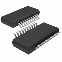
LTC4241CGN#PBF Linear Technology, LTC4241CGN#PBF Datasheet - Page 13

LTC4241CGN#PBF
Manufacturer Part Number
LTC4241CGN#PBF
Description
IC CTRLR HOTSWAP CPCI I2C 20SSOP
Manufacturer
Linear Technology
Type
Hot-Swap Controllerr
Datasheet
1.LTC4241CGN.pdf
(16 pages)
Specifications of LTC4241CGN#PBF
Applications
PCI, PCI-X
Internal Switch(s)
No
Voltage - Supply
3.3V, 5V, ±12V
Operating Temperature
0°C ~ 70°C
Mounting Type
Surface Mount
Package / Case
20-SSOP (0.154", 3.91mm Width)
Input Voltage
12V
Output Voltage
14V
Internal Switch
No
Supply Voltage Range
3.3V To 12V
Digital Ic Case Style
SSOP
No. Of Pins
20
Rohs Compliant
Yes
Lead Free Status / RoHS Status
Lead free / RoHS Compliant
Available stocks
Company
Part Number
Manufacturer
Quantity
Price
APPLICATIO S I FOR ATIO
The current limit and the foldback current level (at the
V
As a design aid, the current limit and foldback level for
commonly used values for R
Table 2. I
The current limit for the internal 12V switch is set at
850mA folding back to 300mA and the –12V switch at
450mA folding back to 200mA.
In systems where it is possible to exceed the current limit
for a short amount of time, it might be necessary to
prevent the analog current loop from responding quickly
so the output voltage does not droop. This can be accom-
plished by adding an RC filter across the sense resistor as
shown in Figure 6. R
offset errors. A capacitor, C
about 1.5 s and a 1 F capacitor gives a delay of about
15 s.
Power-Up/Down Sequence for 3.3V Auxiliary Supply
The 3.3V auxiliary supply is controlled by placing an
external N-channel pass transistor Q3 in the 3.3V
OUT
I
I
LIMIT
FOLDBACK
* ADDITIONAL PINS
R
= 0V) are given by:
OMITTED FOR
CLARITY
SENSE
0.005
0.006
0.007
0.008
0.009
0.01
LIMIT
= 55mV/R
Figure 6. Delay in the Current Limit Loop
( )
and I
= 9mV/R
5V
IN
FOLDBACK
SENSE
5V
3
U
1
IN
17
F
0.007
SENSE
1 F
R1
should be 20 or less to prevent
C
F
5V
vs R
SENSE
U
LTC4241*
I
9.2A
7.9A
6.9A
6.1A
5.5A
2
LIMIT
11A
16
4
R
20
F
F
SENSE
SENSE
, of 0.1 F gives a delay of
IRF7413
GATE 5V
Q1
15
R4
10
W
are given in Table 2.
OUT
18
5V
5A
OUT
I
R7
100
FOLDBACK
C1
0.047 F
1.8A
1.5A
1.3A
1.1A
1.0A
0.9A
U
AUX
power path (Figure 1). The resistor R3 provides load
current fault detection and R6 prevents high frequency
oscillation in Q3.
When power is first applied to V
pulls low. A low-to-high transition at the AUXON pin
initiates the AUXGATE ramp up (Figure 7). The AUXGATE
is pulled high by an internal 10 A current source and the
pass transistor is allowed to turn on. As the auxiliary
controller does not have the foldback current limit feature
and timer control, the inrush supply current during power-
up is limited by ramping the gate of the pass transistor at
a controlled rate (dV/dt = 10 A/C3) where C3 is the total
external capacitance between AUXGATE and ground.
With proper selection of the C3 capacitance value, the
inrush current (I = C
limited to a value less than the current limit set by the sense
resistor R3. This prevents the circuit breaker from tripping
during power-up. C
the 3.3V auxiliary supply line. For example, for C3 = 10nF,
C
current will be 0.47A < I
3.3V
t = (V
A high-to-low transition at the AUXON pin initiates a
AUXGATE ramp-down at a slope of –200 A/C3 as the
AUXGATE is pulled to ground by an internal 200 A current
source. This will allow the load capacitance on the supply
line to discharge while the AUXGATE pulls low to turn off
the external N-channel pass transistor.
LOAD
Figure 7. Power-Up/Down Sequence for 3.3V Auxiliary Supply
AUX
AUXIN
= 470 F, R3 = 0.07 , I
output to reach its final value is equal to
AUXGATE
3.3V
• C3)/10 A.
AUXON
2V/DIV
5V/DIV
2V/DIV
AUX
LOAD
LOAD
is the total load capacitance on
• dV/dt = 10 A • C
LIMIT
5ms/DIV
. The ramp-up time for
LIMIT
AUXIN
= 0.7A, the inrush
, the AUXGATE pin
LTC4241
4241 F07
LOAD
sn4241 4241f
13
/C3) is


