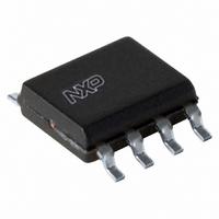
PCA9511AD,112 NXP Semiconductors, PCA9511AD,112 Datasheet - Page 12

PCA9511AD,112
Manufacturer Part Number
PCA9511AD,112
Description
IC HOTSWAP I2C/SMBUS BUFF 8-SOIC
Manufacturer
NXP Semiconductors
Type
I²C-Bus and SMBus Switchr
Datasheet
1.PCA9511ADP118.pdf
(24 pages)
Specifications of PCA9511AD,112
Package / Case
8-SOIC (0.154", 3.90mm Width)
Applications
Hot-Swap/SMB Buffer
Internal Switch(s)
Yes
Current Limit
50mA
Voltage - Supply
2.7 V ~ 5.5 V
Operating Temperature
-40°C ~ 85°C
Mounting Type
Surface Mount
Logic Family
PCA
Maximum Operating Temperature
85 C
Mounting Style
SMD/SMT
Minimum Operating Temperature
- 40 C
Number Of Lines (input / Output)
3 / 3
Propagation Delay Time
70 ns
Logic Type
Bus Buffer
Lead Free Status / RoHS Status
Lead free / RoHS Compliant
Lead Free Status / RoHS Status
Lead free / RoHS Compliant, Lead free / RoHS Compliant
Other names
568-3359-5
935279307112
PCA9511AD
935279307112
PCA9511AD
Available stocks
Company
Part Number
Manufacturer
Quantity
Price
Part Number:
PCA9511AD,112
Manufacturer:
NXP/恩智浦
Quantity:
20 000
NXP Semiconductors
11. Characteristics
Table 5.
V
PCA9511A_4
Product data sheet
Symbol
Power supply
V
I
I
Start-up circuitry
V
V
V
I
t
t
t
t
t
I
C
C
V
Rise time accelerators
I
CC
CC(sd)
I(ENABLE)
en
idle(READY)
dis(EN-RDY)
stp(READY)
READY
LZ(READY)
trt(pu)
CC
CC
pch
IH(ENABLE)
IL(ENABLE)
OL(READY)
i(ENABLE)
o(READY)
= 2.7 V to 5.5 V; T
Characteristics
Parameter
supply voltage
supply current
Shut-down mode supply
current
precharge voltage
HIGH-level input voltage
on pin ENABLE
LOW-level input voltage
on pin ENABLE
input current on pin
ENABLE
enable time
bus idle time to READY
active
disable time (ENABLE to
READY)
SDAIN to READY delay
after STOP
SCLOUT/SDAOUT to
READY delay
off-state leakage current
on pin READY
input capacitance on
pin ENABLE
output capacitance on
pin READY
LOW-level output
voltage on pin READY
transient boosted pull-up
current
amb
= 40 C to +85 V; unless otherwise specified.
Conditions
V
V
V
V
SDA, SCL floating
V
V
V
V
I
positive transition on SDA,
SCL; V
slew rate = 1.25 V/ s
pu
CC
SDAIN
ENABLE
CC
ENABLE
ENABLE
I
I
= V
= V
= 3 mA; V
= 5.5 V;
or GND
CC
CC
CC
= V
= 0 V; all other pins at
= 0 V to V
= V
or GND
or GND
Rev. 04 — 19 August 2009
= 2.7 V;
SCLIN
CC
ENABLE
= 0 V
CC
= V
CC
Hot swappable I
[5][6]
[1]
[1]
[1]
[2]
[1]
[3]
[3]
[4]
[4]
[1]
Min
2.7
-
-
0.8
-
0.3
-
-
50
-
-
-
-
-
-
-
1
V
CC
2
C-bus and SMBus bus buffer
Typ
-
3.5
0.1
1.1
0.5
0.5
110
105
30
1.2
0.8
1.9
2.5
-
2
0.1
0.3
PCA9511A
V
V
CC
CC
© NXP B.V. 2009. All rights reserved.
Max
5.5
6
-
1.2
0.7
-
-
200
-
-
-
-
4.0
4.0
0.4
-
1
V
CC
12 of 24
Unit
V
mA
V
V
V
ns
pF
pF
V
mA
A
A
s
s
s
s
A


