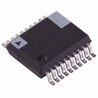
ADE7760ARSRL Analog Devices Inc, ADE7760ARSRL Datasheet - Page 7

ADE7760ARSRL
Manufacturer Part Number
ADE7760ARSRL
Description
IC ENERGY METER W/OCFD 20SSOP TR
Manufacturer
Analog Devices Inc
Datasheet
1.ADE7760ARS.pdf
(24 pages)
Specifications of ADE7760ARSRL
Rohs Status
RoHS non-compliant
Input Impedance
400 KOhm
Measurement Error
0.1%
Voltage - I/o High
2.4V
Voltage - I/o Low
0.8V
Current - Supply
4mA
Voltage - Supply
4.75 V ~ 5.25 V
Operating Temperature
-40°C ~ 85°C
Mounting Type
Surface Mount
Package / Case
20-SSOP (0.200", 5.30mm Width)
Meter Type
Single Phase
Lead Free Status / Rohs Status
Not Compliant
TERMINOLOGY
Measurement Error
The error associated with the energy measurement made by the
ADE7760 is defined by the following formula:
Phase Error between Channels
The high-pass filter (HPF) in the current channel has a phase
lead response. To offset this phase response and equalize the
phase response between channels, a phase correction network is
also placed in the current channel. The phase correction net-
work ensures a phase match between the current channels and
voltage channels to within ±0.1° over a range of 45 Hz to 65 Hz
and ±0.2° over a range 40 Hz to 1 kHz.
Power Supply Rejection
This quantifies the ADE7760 measurement error as a percent-
age of reading when the power supplies are varied. For the ac
PSR measurement, a reading at nominal supplies (5 V) is taken.
A second reading is obtained with the same input signal levels
when an ac (175 mV rms/100 Hz) signal is introduced onto the
supplies. Any error introduced by this ac signal is expressed as a
percentage of reading (see the Measurement Error definition
above).
Percentage
⎛
⎜
⎜
⎝
Energy
registered
Error
True
=
by
ADE
Energy
7760
−
True
Energy
×
100
%
⎞
⎟
⎟
⎠
Rev. 0 | Page 7 of 24
For the dc PSR measurement, a reading at nominal supplies
(5 V) is taken. A second reading is obtained with the same input
signal levels when the power supplies are varied ±5%. Any error
introduced is again expressed as a percentage of reading.
ADC Offset Error
This refers to the dc offset associated with the analog inputs to
the ADCs. It means that with the analog inputs connected to
AGND the ADCs still see a dc analog input signal. The magni-
tude of the offset depends on the input range selection (see the
Typical Performance Characteristics section). However, when
HPFs are switched on, the offset is removed from the current
channels and the power calculation is not affected by this offset.
Gain Error
The gain error in the ADE7760 ADCs is defined as the differ-
ence between the measured output frequency (minus the offset)
and the ideal output frequency. The difference is expressed as a
percentage of the ideal frequency. The ideal frequency is
obtained from the transfer function (see the Transfer Function
section).
ADE7760


