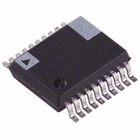
ADE7760ARSRL Analog Devices Inc, ADE7760ARSRL Datasheet - Page 16

ADE7760ARSRL
Manufacturer Part Number
ADE7760ARSRL
Description
IC ENERGY METER W/OCFD 20SSOP TR
Manufacturer
Analog Devices Inc
Datasheet
1.ADE7760ARS.pdf
(24 pages)
Specifications of ADE7760ARSRL
Rohs Status
RoHS non-compliant
Input Impedance
400 KOhm
Measurement Error
0.1%
Voltage - I/o High
2.4V
Voltage - I/o Low
0.8V
Current - Supply
4mA
Voltage - Supply
4.75 V ~ 5.25 V
Operating Temperature
-40°C ~ 85°C
Mounting Type
Surface Mount
Package / Case
20-SSOP (0.200", 5.30mm Width)
Meter Type
Single Phase
Lead Free Status / Rohs Status
Not Compliant
ADE7760
The output frequency on CF can be up to 2048 times higher
than the frequency on F1 and F2. This higher output frequency
is generated by accumulating the instantaneous active power
signal over a much shorter time while converting it to a
frequency. This shorter accumulation period means less
averaging of the cos(2ωt) component. As a consequence, some
of this instantaneous power signal passes through the digital-to-
frequency conversion. This is not a problem in the application.
Where CF is used for calibration purposes, the frequency
should be averaged by the frequency counter, which removes
any ripple. If CF is being used to measure energy, such as in a
microprocessor-based application, the CF output should also be
averaged to calculate power. Because the outputs F1 and F2
operate at a much lower frequency, a lot more averaging of the
instantaneous active power signal is carried out. The result is a
greatly attenuated sinusoidal content and a virtually ripple-free
frequency output.
TRANSFER FUNCTION
Frequency Outputs F1 and F2
The ADE7760 calculates the product of two voltage signals (on
Channel 1 and Channel 2) and then low-pass filters this product
to extract active power information. This active power
information is then converted to a frequency. The frequency
information is output on F1 and F2 in the form of active high
pulses. The pulse rate at these outputs is relatively low, for
example, 0.34 Hz maximum for ac signals with S0 = S1 = 0
(see Table 7). This means that the frequency at these outputs is
generated from active power information accumulated over a
relatively long period of time. The result is an output frequency
that is proportional to the average active power. The averaging
of the active power signal is implicit to the digital-to-frequency
conversion. The output frequency or pulse rate is related to the
input voltage signals by the following equation:
where:
F
V1
V2
V
F
logic inputs S0 and S1 (see Table 5).
1
1–4
REF
− F
rms
rms
is one of four possible frequencies selected by using the
is the reference voltage (2.5 V ± 8%) (V).
F
is the differential rms voltage signal on Channel 1 (V).
is the differential rms voltage signal on Channel 2 (V).
2
1
Frequency is the output frequency on F1 and F2 (Hz).
−
F
2
Frequency
=
. 5
70
×
V1
rms
V
REF
×
V2
2
rms
×
F
1
−
4
(7)
Rev. 0 | Page 16 of 24
Table 5. F
S1
0
0
1
1
1
2
Frequency Output CF
The pulse output calibration frequency (CF) is intended for use
during calibration. The output pulse rate on CF can be up to
2048 times the pulse rate on F1 and F2. The lower the F
frequency selected, the higher the CF scaling. Table 6 shows
how the two frequencies are related, depending on the states of
the logic inputs S0, S1, and SCF. Because of its relatively high
pulse rate, the frequency at this logic output is proportional to
the instantaneous active power. As with F1 and F2, the fre-
quency is derived from the output of the low-pass filter after
multiplication. However, because the output frequency is high,
this active power information is accumulated over a much
shorter time. Therefore, less averaging is carried out in the
digital-to-frequency conversion. With much less averaging of
the active power signal, the CF output is much more responsive
to power fluctuations (see Figure 17).
Table 6. Relationship between CF and F1, F2 Frequency
Outputs
SCF
1
0
1
0
1
0
1
0
Example
In this example, if ac voltages of ±660 mV peak are applied to
V1 and V2, then the expected output frequency on CF, F1, and
F2 is calculated as follows:
F
V1
V2
V
Values are generated using the nominal frequency of 450 kHz.
F
internal oscillator frequency (OSC).
1–4
REF
1–4
rms
rms
are a binary fraction of the master clock and, therefore, varies, if the
= 1.7 Hz, SCF = S1 = S0 = 0
= 2.5 V (nominal reference value)
= rms of 660 mV peak ac = 0.66/√ 2 V
= rms of 660 mV peak ac = 0.66/√ 2 V
S1
0
0
0
0
1
1
1
1
1–4
S0
0
1
0
1
Frequency Solution
S0
0
0
1
1
0
0
1
1
F
1.72
1.72
3.44
3.44
6.86
6.86
13.7
13.7
F
1.72
3.44
6.86
13.7
1–4
1–4
(Hz)
(Hz)
1
CF Frequency Output
128 × F1, F2
64 × F1, F2
64 × F1, F2
32 × F1, F2
32 × F1, F2
16 × F1, F2
16 × F1, F2
2048 × F1, F2
OSC/CLKIN
OSC/2
OSC/2
OSC/2
OSC/2
18
17
16
15
2
1–4


