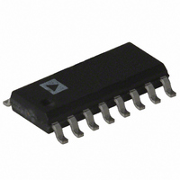
ADE7757ARN Analog Devices Inc, ADE7757ARN Datasheet - Page 2

ADE7757ARN
Manufacturer Part Number
ADE7757ARN
Description
IC ENERGY METERING 16-SOIC
Manufacturer
Analog Devices Inc
Datasheet
1.ADE7757ARNZ.pdf
(16 pages)
Specifications of ADE7757ARN
Rohs Status
RoHS non-compliant
Input Impedance
320 KOhm
Measurement Error
0.1%
Voltage - I/o High
2.4V
Voltage - I/o Low
0.8V
Current - Supply
5mA
Voltage - Supply
4.75 V ~ 5.25 V
Operating Temperature
-40°C ~ 85°C
Mounting Type
Surface Mount
Package / Case
16-SOIC (0.154", 3.90mm Width)
Meter Type
Single Phase
Available stocks
Company
Part Number
Manufacturer
Quantity
Price
Part Number:
ADE7757ARNZ
Manufacturer:
ADI/亚德诺
Quantity:
20 000
Part Number:
ADE7757ARNZRL
Manufacturer:
ADI/亚德诺
Quantity:
20 000
ADE7757–SPECIFICATIONS
Parameter
ACCURACY
ANALOG INPUTS
OSCILLATOR FREQUENCY (OSC)
REFERENCE INPUT
ON-CHIP REFERENCE
LOGIC INPUTS
LOGIC OUTPUTS
POWER SUPPLY
NOTES
1
2
3
Specifications subject to change without notice.
See Terminology section for explanation of specifications.
See plots in Typical Performance Characteristics.
Sample tested during initial release and after any redesign or process change that may affect this parameter.
Measurement Error
Phase Error
AC Power Supply Rejection
DC Power Supply Rejection
Channel V1 Maximum Signal Level
Channel V2 Maximum Signal Level
Input Impedance (DC)
Bandwidth (–3 dB)
ADC Offset Error
Gain Error
Oscillator Frequency Tolerance
Oscillator Frequency Stability
REF
Input Capacitance
Reference Error
Temperature Coefficient
SCF, S0, S1,
F1 and F2
CF
V
I
DD
DD
V1 Phase Lead 37
(PF = 0.8 Capacitive)
V1 Phase Lag 60
(PF = 0.5 Inductive)
Output Frequency Variation (CF)
Output Frequency Variation (CF)
Input High Voltage, V
Input Low Voltage, V
Input Current, I
Input Capacitance, C
Output High Voltage, V
Output Low Voltage, V
Output High Voltage, V
Output Low Voltage, VOL
Frequency Output Error
IN/OUT
1
Input Voltage Range
1, 2
1
between Channels
3
1, 2
3
IN
1
on Channel V1
IN
INL
INH
OL
OH
OH
1, 2
1
1
1
(CF)
1
Value
0.1
0.2
320
7
450
2.7
2.3
10
2.4
0.8
10
4.5
0.5
4
0.5
4.75
5.25
5
0.1
0.1
0.3
30
165
18
4
12
30
200
20
1
10
Unit
% Reading typ
Degrees ( ) max
Degrees ( ) max
% Reading typ
% Reading typ
mV max
mV max
k min
kHz nominal
mV max
% Ideal typ
kHz nominal
% Reading typ
ppm/ C typ
V max
V min
pF max
mV max
ppm/ C typ
V min
V max
pF max
V min
V max
V min
V max
% Ideal typ
V min
V max
mA max
A max
(V
0.5%
DD
= 5 V
50 ppm/ C, T
–2–
5%, AGND = DGND = 0 V, On-Chip Reference, RCLKIN = 6.2 k ,
Test Conditions/Comments
Channel V2 with Full-Scale Signal ( 165 mV), 25 C
Over a Dynamic Range 500 to 1
Line Frequency = 45 Hz to 65 Hz
S0 = S1 = 1,
V1 = 21.2 mV rms, V2 = 116.7 mV rms @ 50 Hz
Ripple on V
S0 = S1 = 1,
V1 = 21.2 mV rms, V2 = 116.7 mV rms,
V
See Analog Inputs section
V1P and V1N to AGND
V2P and V2N to AGND
OSC = 450 kHz, RCLKIN = 6.2 k , 0.5%
OSC = 450 kHz, RCLKIN = 6.2 k , 0.5%
See Terminology Section and Typical Performance Characteristics
External 2.5 V Reference
V1 = 21.2 mV rms, V2 = 116.7 mV rms
RCLKIN = 6.2 k , 0.5%
2.5 V + 8%
2.5 V – 8%
Nominal 2.5 V
V
V
Typically 10 nA, V
I
V
I
V
I
V
I
V
External 2.5 V Reference,
V1 = 21.2 mV rms, V2 = 116.7 mV rms
For Specified Performance
5 V – 5%
5 V + 5%
Typically 4 mA
SOURCE
SINK
SOURCE
SINK
DD
DD
DD
DD
DD
DD
DD
= 5 V
= 5 V
= 5 V
= 5 V
= 5 V
= 5 V
= 5 V
= 10 mA
= 5 mA
MIN
= 10 mA
= 5 mA
to T
DD
250 mV
5%
5%
MAX
of 200 mV rms @ 100 Hz
= –40 C to +85 C, unless otherwise noted.)
IN
= 0 V to V
50 ppm/ C
DD
5
50 ppm/ C
0
ppm/ C
REV. A


