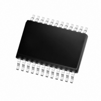
MCP3909-I/SS Microchip Technology, MCP3909-I/SS Datasheet - Page 5

MCP3909-I/SS
Manufacturer Part Number
MCP3909-I/SS
Description
IC POWER METERING-1 PHASE 24SSOP
Manufacturer
Microchip Technology
Datasheets
1.MCP3909T-ISS.pdf
(44 pages)
2.MCP3909T-ISS.pdf
(104 pages)
3.MCP3909-ISS.pdf
(40 pages)
Specifications of MCP3909-I/SS
Package / Case
24-SSOP (0.200", 5.30mm Width)
Input Impedance
390 KOhm
Measurement Error
0.1%
Voltage - I/o High
2.4V
Voltage - I/o Low
0.85V
Current - Supply
2.3mA
Voltage - Supply
4.5 V ~ 5.5 V
Operating Temperature
-40°C ~ 85°C
Mounting Type
Surface Mount
Meter Type
Single Phase
Operating Temperature Range
- 40 C to + 85 C
Mounting Style
SMD/SMT
Supply Voltage Range
4.5V To 5.5V
Digital Ic Case Style
SSOP
No. Of Pins
24
Interface Type
Serial, SPI
Supply Voltage Max
5.5V
Rohs Compliant
Yes
Lead Free Status / RoHS Status
Lead free / RoHS Compliant
For Use With
MCP3909EV-MCU16 - EVALUATION BOARD FOR MCP3909MCP3909RD-3PH1 - REF DESIGN MCP3909 3PH ENGY MTR
Lead Free Status / Rohs Status
Lead free / RoHS Compliant
Available stocks
Company
Part Number
Manufacturer
Quantity
Price
Part Number:
MCP3909-I/SS
Manufacturer:
MICROCHIP/微芯
Quantity:
20 000
© 2006 Microchip Technology Inc.
TIMING CHARACTERISTICS
Electrical Specifications: Unless otherwise indicated, all parameters apply at AV
A
Frequency Outputs
F
(Logic Low)
HF
F
HF
F
Time
F
ration
Digital I/O
F
Voltage
F
Voltage
HF
Voltage
HF
Voltage
High-Level Input Voltage
(All Digital Input Pins)
Low Level Input Voltage
(All Digital Input Pins)
Input Leakage Current
Pin Capacitance
Serial Interface Timings (Note 4)
Output Data Rate
Serial Clock Frequency
Window for serial mode entry
codes
Window start time for serial
mode entry codes
Serial Clock High Time
Serial Clock Low Time
CS Fall to First Rising CLK Edge
Data Input Setup Time
Data Input Hold Time
CS Rise to Output Disable
CLK Fall to Output Data Valid
Note 1:
OUT0
OUT0
OUT0
OUT0
OUT0
OUT0
GND
OUT
OUT
OUT
OUT
, D
2:
3:
4:
and F
and F
to F
to F
and F
and F
Pulse Width
Pulse Period
and NEG Output High
and NEG Output Low
GND
Parameter
OUT1
OUT1
If output pulse period (t
If output pulse period (t
equals 0,1,1, the HF
Specified by characterization, not production tested.
Serial timings specified and production tested with 180 pF load.
OUT1
OUT1
OUT1
OUT1
= 0V, MCLK = 3.58 MHz; T
Falling-Edge
Minimum Sepa-
Pulse Width
Pulse Period
Output High
Output Low
OUT
FP
HP
t
t
WINDOW
WINSET
pulse time is fixed at 64 x MCLK periods or 18 µs for MCLK = 3.58 MHz
t
f
Sym
) falls below 984376*2 MCLK periods, then t
SUCS
) falls below 322160*2 MCLK periods, then t
t
V
V
f
t
V
V
t
t
V
ADC
t
t
V
t
t
t
t
t
CLK
FS2
t
FW
HW
DIS
HP
SU
HD
DO
FP
FS
LO
OH
OH
OL
OL
HI
IH
IL
A
= -40°C to +85°C.
1/MCLK
Min
4.5
4.5
2.4
10
30
15
10
—
—
—
—
—
—
—
—
—
—
—
—
—
—
Refer to
Refer to
MCLK/256
4/MCLK
0.5 t
Equation 4-1
Equation 4-2
Typ
275
0.1
90
—
—
—
—
—
—
—
—
—
—
—
—
—
—
—
—
—
FP
8/MCLK
Max
0.85
150
0.5
0.5
10
20
20
10
30
±1
—
—
—
—
—
—
—
—
—
—
—
40
Units
MHz
FW
HW
ms
ms
µA
pF
ns
ns
ns
ns
ns
ns
ns
—
—
DD
V
V
V
V
V
V
s
s
= 1/2 t
= 1/2 t
= DV
984376 MCLK periods
(Note 1)
322160 MCLK periods
(Note 2)
I
I
I
I
DV
DV
V
(Note 3)
V
Last bit must be clocked in
before this time.
First bit must be clocked in
after this time.
OH
OL
OH
OL
DD
IN
DD
FP
HP
DD
DD
= 12 mA, DV
= 12 mA, DV
.
MCP3909
= 0, V
= 12 mA, DV
= 12 mA, DV
. When F2, F1, F0
= 4.5V to 5.5V,
= 5V
= 5.0V
= 5.0V
Comment
IN
DS22025A-page 5
= DV
DD
DD
DD
DD
DD
= 5.0V
= 5.0V
= 5.0V
= 5.0V


